 +86 755 2794 4155
  sales@knownpcb.com
-
Shenzhen KNOWNPCB Technology Co., Ltd.
 +86 755 2794 4155
  sales@knownpcb.com
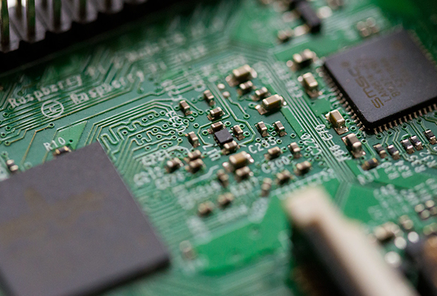
Have you noticed that now more and more of our lighting is using led lighting.What is LED? Compared to the traditional light bulbs, LEDs have lower power consumption, longer lifetime and higher energy efficiency. In the PCB industry,when we say LED PCB, it refers to the pcb used for LED lighting, if you are looking for a suitable LED PCB for your lighting system, this article may bring you something. WHAT ARE LEDS COMPOSED OF?LED is an initial light-emitting diode that produces light when an electric current passes through. LEDs typically have negative and positive electrodes, which generate light in the visible light region.The LEDS are glued to the PCB by soldering process and have electrical connections for lighting.Since light-emitting diodes dissipate a lot of heat when they are in use, when you are designing LED, the metal core is usually the best choice for LED PCB, it is because that it dissipates heat more faster. Among them, the metal material aluminum is the most widely used
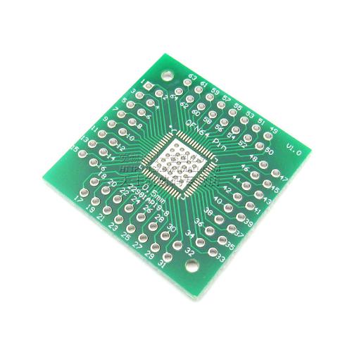
PCBA is the entire process of SMT loading through PCB empty boards, followed by DIP plugins; Placement and welding are the core processes in PCBA. So, what are the requirements for chip mounting and welding in the PCBA processing process? 1、 PCBA SMT processing process requirements: 1. Based on customer Gerber files and BOM sheets, create SMT production process files and generate SMT coordinate files. 2. Check if all production materials are ready and confirm the PMC plan for production. 3. Conduct SMT programming and create a homepage for verification. 4. According to the SMT process, make laser steel mesh. 5. Perform solder paste printing to ensure that the printed solder paste is uniform and of good thickness. 6. Mount the components onto the circuit board using an SMT mounting machine, and perform online AOI testing if necessary. 7. Set a perfect reflow soldering furnace temperature curve to allow the circuit board to flow through reflow soldering, and the solder paste
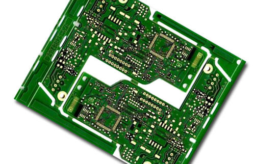
Many beginners are always confused about the rules and requirements for PCB circuit board sampling fees. What materials do they need to provide? Let the engineer explain this process to you: 1、 How much do I charge for PCB sampling? Firstly, it depends on what type of board is used, such as FR4, high TG board, and brand benefits. The plates are different, and the prices are also different. In addition, according to the design drawings, the smaller the line width and spacing, the more holes there are, and the more precise it is, the higher the cost. Looking at the surface treatment, sinking gold and gilding are more expensive than tin and OSP. Four Look at Quantity . According to the delivery date, PCB boards that require expedited delivery are cheaper than those that require regular delivery. 2、 What do I need to provide for PCB sampling? Information that needs to be provided to the manufacturer for quotation, drawings generally provide GEBER documents, with clear process requ
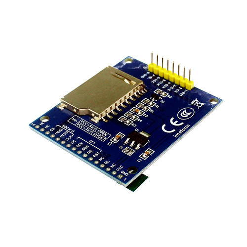
With the development of PCB technology towards high density and refinement, the role of multi-layer PCB boards is becoming increasingly important and widely used in various fields. Below is the engineer's interpretation of several common questions about multi-layer PCB circuit boards: 1. How many layers can a multi-layer PCB board have at most? PCB boards were initially mainly composed of single or double panels, but later with the development of technology, multi-layer PCB boards were needed to achieve the interaction of multi-layer circuits. Components range from simple single sided boards to 4, 6, 8, 10, 12, and even 22 or more layers. There is no conclusion regarding the maximum number of layers on a multi-layer PCB board. For research and development institutions, the number of layers of a PCB depends on the product requirements and functions implemented by the electronic PCB application. 2. Is it better to have more layers of multi-layer PCB boards? Generally speaking, the
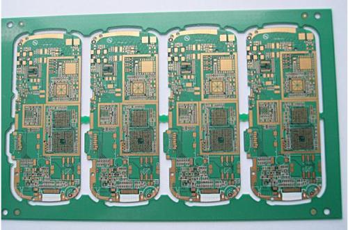
PCB ink plays a role in protecting the copper foil during the production of PCB circuit boards, preventing the copper skin from being exposed, thereby affecting the subsequent processes; The commonly used ink colors are white oil, green oil, black oil, blue oil, red oil, and butter. So, what are the precautions for using PCB ink? In any case, the temperature of the ink must be maintained between 20-25 ℃, otherwise it will affect the viscosity of the ink and the quality and effectiveness of screen printing. Especially when ink is stored outdoors or at different temperatures, it must be placed at ambient temperature for a few days before reuse or until the ink barrel reaches the appropriate temperature for use. 2. Before use, the ink must be thoroughly and carefully mixed manually or mechanically. If air enters the ink, it should be left to stand for a period of time before use; If dilution is required, first mix thoroughly and then test its viscosity. The ink bucket must be sealed
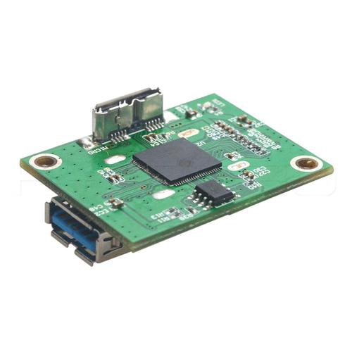
Many newcomers often confuse nickel palladium plating with nickel gold plating. So, what is the difference between PCB sample nickel palladium plating and nickel gold plating? Nickel palladium plating is a non selective surface processing process that involves depositing a layer of nickel, palladium, and gold onto the surface of the copper layer of the printed circuit using chemical methods in PCB sampling. Electroplating nickel gold refers to the process of making gold particles adhere to PCB boards through electroplating, which is also known as hard gold due to its strong adhesion; This process can greatly increase the hardness and wear resistance of PCBs, effectively preventing the diffusion of copper and other metals. The difference between chemical nickel palladium gold and electroplating nickel gold: Similarities: 1. Both belong to important surface treatment processes in PCB sampling; 2. The main application field is wiring and connection technology, which is suitable
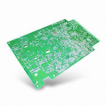
Aluminum substrate is a metal based copper clad plate with good thermal conductivity, electrical insulation performance, and mechanical processing performance. Let the Shenzhen PCB manufacturer take you to understand what aluminum substrates are. 1、 Characteristics of aluminum substrate 1. Adopting surface mount technology; 2. Extremely effective treatment of thermal diffusion; 3. Reduce product operating temperature, improve product power density and reliability; 4. Reduce product volume and assembly costs; 5. Replace fragile ceramic substrates. 2、 Structure of aluminum substrate The aluminum substrate consists of copper foil, thermal insulation layer, and metal substrate: Copper foil: The thickness of the copper foil for the circuit is between loz and 10oz. Thermal insulation layer: It is a low thermal resistance thermal insulation material. Metal substrate: generally aluminum based copper clad plate and traditional epoxy glass cloth laminated plate. Explanation: 1.
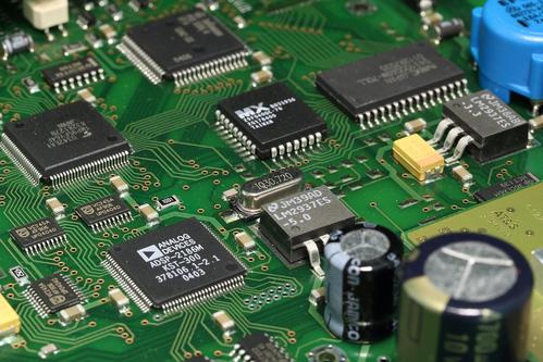
PCB circuit boards are prone to malfunctions during use, which involves maintenance. So, what are the issues to pay attention to when repairing PCB circuit boards? 1、 Understand the vulnerable components on the circuit board 1. Areas with unreasonable design are most prone to malfunctions Firstly, there is a heat dissipation issue, as many PCB boards are damaged due to poor heat dissipation design; Secondly, there is copper foil wire. The copper foil of circuit board power lines with poor quality is very thin and easily burnt out due to overcurrent. 2. Frequently used areas are prone to malfunctions For example, the drive motor of the circuit board, the shaft, the switch tube of the switching power supply, the operation panel, etc. 3. Components with heavy loads, high power, and high operating voltage are most likely to malfunction The power supply, driving circuit, power control device, operational amplifier, etc. of the circuit board are the most easily damaged. 4. Protec
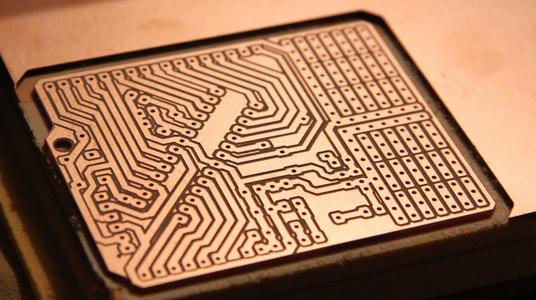
The anti-interference ability of PCB circuit boards can affect the effective performance of electronic devices, and the anti-interference ability of PCB circuit boards is closely related to specific circuits. So, what are the anti-interference measures for PCB circuit boards? 1. Principle of ground wire design: If there are both logical and linear circuits on the PCB circuit board, they should be separated as much as possible; The grounding of low-frequency circuits should be connected in parallel with a single point as much as possible. If there are difficulties in actual wiring, partial series connection can be used before connecting to the ground. 2. Closed loop composed of grounding wires: PCB circuit boards composed solely of digital circuits, with their grounding circuits arranged in a clustered loop, can mostly improve their noise resistance. 3. On the premise that the speed can meet the requirements, try to reduce the crystal oscillator of the microcontroller and select lo
Inquiry Now

