 +86 755 2794 4155
  sales@knownpcb.com
-
Shenzhen KNOWNPCB Technology Co., Ltd.
 +86 755 2794 4155
  sales@knownpcb.com
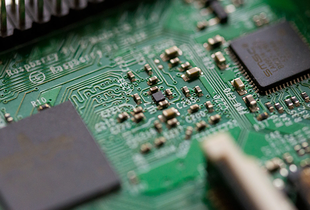
Have you noticed that now more and more of our lighting is using led lighting.What is LED? Compared to the traditional light bulbs, LEDs have lower power consumption, longer lifetime and higher energy efficiency. In the PCB industry,when we say LED PCB, it refers to the pcb used for LED lighting, if you are looking for a suitable LED PCB for your lighting system, this article may bring you something. WHAT ARE LEDS COMPOSED OF?LED is an initial light-emitting diode that produces light when an electric current passes through. LEDs typically have negative and positive electrodes, which generate light in the visible light region.The LEDS are glued to the PCB by soldering process and have electrical connections for lighting.Since light-emitting diodes dissipate a lot of heat when they are in use, when you are designing LED, the metal core is usually the best choice for LED PCB, it is because that it dissipates heat more faster. Among them, the metal material aluminum is the most widely used
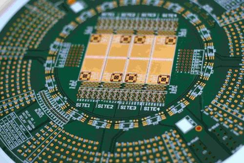
In the field of PCB, there are often many English terms that industry insiders may find difficult to fully recognize. How much do you know about PCB terminology? Let me introduce some commonly used terms in the PCB field to you: 1. FR4 In most cases, the glass fiber substrate for PCBs generally refers to the material "FR4". The solid material "FR4" gives PCB hardness and thickness. Some cheap PCBs are made of materials such as epoxy resin or phenol, lacking the durability of FR4, but they are much cheaper. Phenolic substances have a lower thermal decomposition temperature, and excessive welding time can lead to their decomposition and carbonization, and emit unpleasant odors. 2. Copper The thin copper foil layer on a PCB is pressed onto the substrate through heat and adhesive during production. On double-sided boards, copper foil is pressed onto both sides of the substrate. When we mention "double-sided board" or "two-layer board", we refer to two layers of copper foil on a th
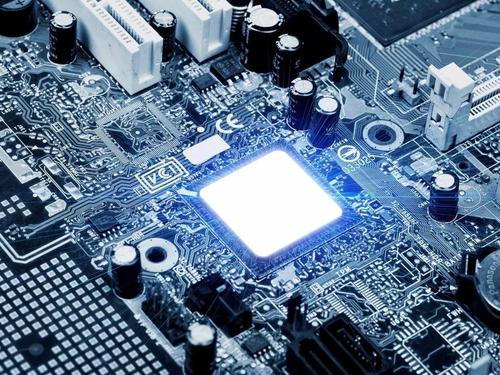
Soft hard combination board refers to a circuit board with FPC and PCB characteristics that is formed by combining flexible circuit boards and hard circuit boards in PCB sampling through pressing and other processes according to relevant process requirements. So, what are the application areas of soft and hard combination boards? 1. Industrial use: including industrial, military, and medical fields. The requirements for soft and hard boards in these fields include high reliability, high accuracy, low impedance loss, complete signal transmission quality, and durability. Due to the complexity of the manufacturing process and low output, the production cost is high. 2. Mobile phone: The application of a soft and hard combination board in a mobile phone, commonly including the turning point of a foldable phone, image module, buttons, and RF module. 3. Consumer electronics products: The software and hardware boards used in DSC and DV are the most representative. In terms of performan
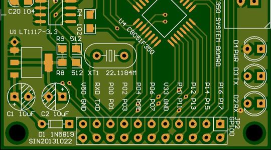
Copper clad laminate (CCL) is the most widely used and important basic board for PCB sampling; It consists of three parts: copper foil, reinforcing material, and adhesive. Its function is to support various components and achieve electrical connections or insulation between them. So, what are the classifications of PCB foil plates? 1. Classification by reinforcement material The most commonly used reinforcement materials for laminated sheets are alkali free, fiberglass products, or paper. Therefore, laminates can be divided into two categories: glass cloth based and paper based. 2. Classification by adhesive type The main adhesives used for laminated sheets include phenolic, epoxy, polyester, polyimide, polytetrafluoroethylene resin, etc. Therefore, laminated sheets are also divided into phenolic, epoxy, polyester, polyimide, and polytetrafluoroethylene laminated sheets accordingly. 3. Classification based on substrate characteristics and usage According to the degree of comb

The so-called copper coating refers to using the idle space on the PCB as a reference plane, and then filling it with solid copper. These copper areas are also known as copper filling. Copper coating can be divided into large-area copper coating and grid copper coating. Next, let professional PCB manufacturers provide you with a detailed understanding of the basic knowledge of PCB circuit board copper coating: 1、 Precautions for copper coating: 1. Single point connection in different locations: connected through a 0 ohm resistor, magnetic bead, or inductor. 2. The copper coating near the crystal oscillator is used as a high-frequency emission source in the circuit. The crystal oscillator should be surrounded by copper coating, and then the outer shell of the crystal oscillator should be grounded separately. 2、 What are the benefits of copper coating? 1. Copper coating can reduce ground wire impedance and improve anti-interference ability; 2. Reduce voltage drop and improve po
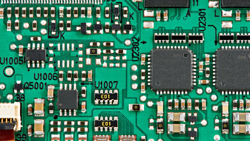
The reasons for the warping of printed circuit boards are, on one hand, the possible warping of the substrate used, and on the other hand, the warping caused by thermal stress, chemical factors, and improper processing during the processing. So, what are the preventive measures for warping of printed circuit boards? 1. Prevent improper inventory methods from causing substrate warping. (1) During the storage process, if the humidity in the inventory environment is high, the copper clad plate will increase warping due to moisture absorption. So for copper clad panels without moisture-proof packaging, attention should be paid to warehouse conditions, minimize warehouse humidity, and avoid bare placement of copper clad panels. (2) Improper placement of copper clad panels can increase warping. If placed vertically or with heavy objects pressed on the copper clad plate, it will increase the warping deformation. Solution: Improve the storage environment, eliminate vertical placement,
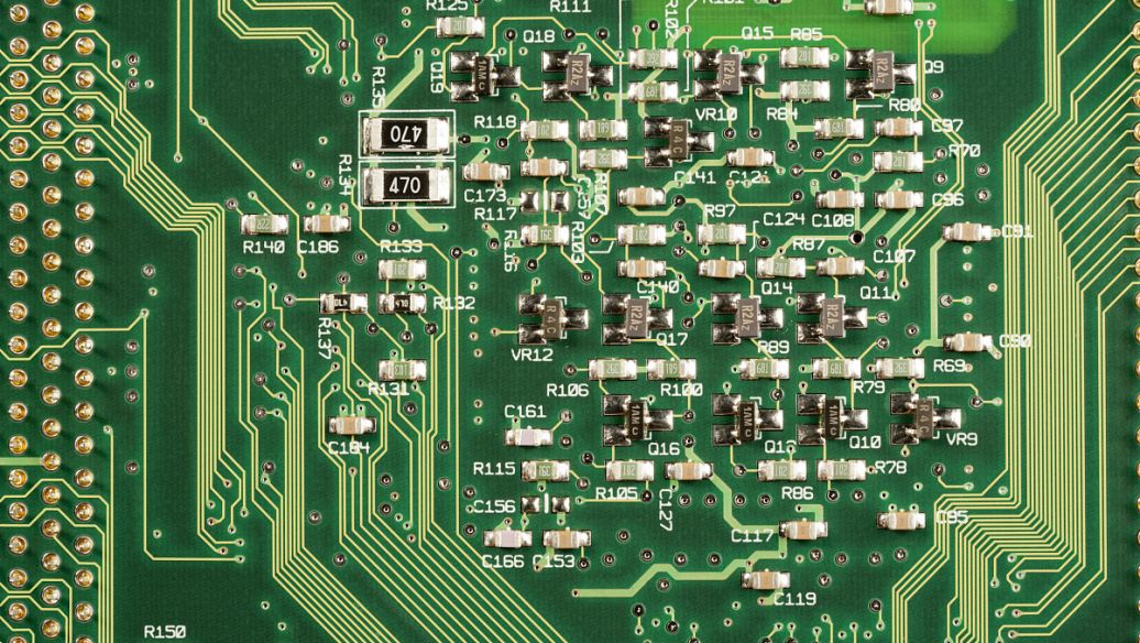
PCB wiring is very important and has a significant impact on the product's lifespan, stability, and electromagnetic compatibility. If the wiring of the circuit board is unreasonable, the product performance will be greatly reduced. Below, we will introduce several special methods for PCB circuit board wiring, hoping to be helpful to you. 1. Right angle wiring: The impact of right angle routing on signals is mainly reflected in: (1) Corners can be equivalent to capacitive loads on the transmission line, slowing down the rise time; (2) Impedance discontinuity can cause signal reflection; (3) The EMI generated by the right angled tip will become a focus of high-speed circuit design in the field of RF design above 10GHz. 2. Differential wiring The advantages of differential signal compared to ordinary single ended signal wiring are as follows: (1) Strong anti-interference ability. Because the coupling between two differential routing lines is good, when there is external noise
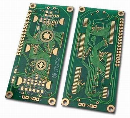
PCB design is particularly important as it appears in almost every electronic device. So, what are the common mistakes in PCB circuit board design? 1、 Character shuffling Including character cover solder pads and SMD solder pads, which brings inconvenience to printed board testing and component welding; The character design is too small, making it difficult to screen, and it can cause characters to overlap and be difficult to distinguish. 2、 Abuse of graphic layers 1. Some useless connections were made on some graphics layers. 2. When designing, it is easy to draw and label the lines that are common to each layer using the Board layer. However, when conducting photo data, the circuit is broken due to missing lines due to the absence of a Board layer. 3、 Overlap of pads 1. The overlap of solder pads (excluding surface mounted solder pads) means the overlap of holes, which can cause damage to the holes during the drilling process due to multiple drilling at one location. 2. T
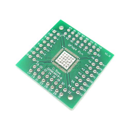
PCB is the fundamental electronic component of all electronic circuit designs, and the design of PCB circuit boards is also a must for engineers to understand. So, what methods should be mastered in PCB circuit board design? 1. There should be a reasonable direction The best direction is in a straight line, but it is generally not easy to achieve, and the most unfavorable direction is in a circular shape. For input/output, AC/DC, strong/weak signals, high-frequency/low-frequency, high-voltage/low-voltage, etc., their direction should be linear (or separated) and should not blend with each other, with the aim of preventing mutual interference. 2. Choose a good grounding point In general, it is required to have a common ground connection, such as: the multiple ground wires of the forward amplifier should be merged and then connected to the main ground, etc. In reality, it is difficult to fully achieve due to various limitations, but efforts should be made to follow them. 3. Reas
Inquiry Now

