 +86 755 2794 4155
  sales@knownpcb.com
-
Shenzhen KNOWNPCB Technology Co., Ltd.
 +86 755 2794 4155
  sales@knownpcb.com
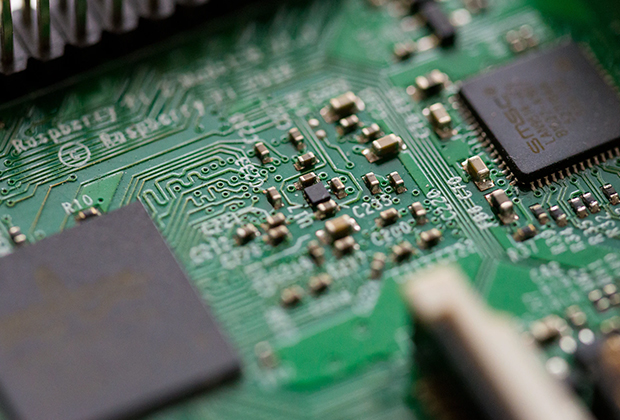
Have you noticed that now more and more of our lighting is using led lighting.What is LED? Compared to the traditional light bulbs, LEDs have lower power consumption, longer lifetime and higher energy efficiency. In the PCB industry,when we say LED PCB, it refers to the pcb used for LED lighting, if you are looking for a suitable LED PCB for your lighting system, this article may bring you something. WHAT ARE LEDS COMPOSED OF?LED is an initial light-emitting diode that produces light when an electric current passes through. LEDs typically have negative and positive electrodes, which generate light in the visible light region.The LEDS are glued to the PCB by soldering process and have electrical connections for lighting.Since light-emitting diodes dissipate a lot of heat when they are in use, when you are designing LED, the metal core is usually the best choice for LED PCB, it is because that it dissipates heat more faster. Among them, the metal material aluminum is the most widely used
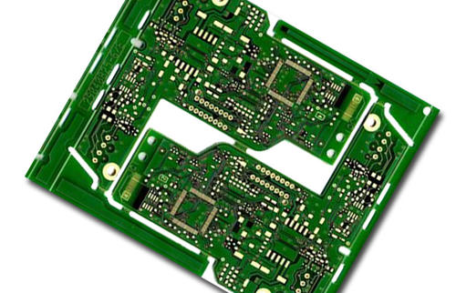
High frequency PCB circuit design is a very complex design process, and its wiring is crucial for the entire design! So, what are the wiring methods for high-frequency PCB circuits? 1. Multilayer board wiring In the PCB layout stage, choose a reasonable number of layers of printed circuit board size, fully utilize the middle layer to set shielding, better achieve nearby grounding, effectively reduce parasitic inductance and shorten signal transmission length, while also significantly reducing signal cross interference. 2. The less bent the leads between electronic device pins, the better It is best to use a full straight line as the lead wire, which requires a turning point. A 45 degree broken line or arc turning point can be used to meet this requirement, but it can reduce the external emission and mutual coupling of high-frequency signals. 3. The shorter the lead between device pins, the better The radiation intensity of a signal is directly proportional to the length of th
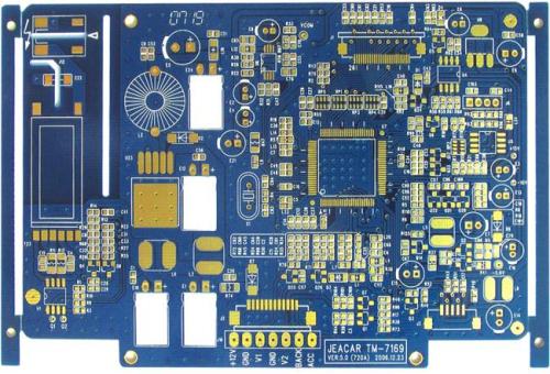
There are significant differences in the usage scenarios, products, performance, materials, areas, and other aspects of PCB boards, resulting in significant changes in the types of components used, the thickness of connecting wires, and the density of wiring. So, what factors need to be considered when selecting PCB boards? 1. For general electronic products, use FR4 epoxy glass fiber substrate; For use with high ambient temperatures or flexible circuit boards, polyimide glass fiber substrates are used; For high-frequency boards, polytetrafluoroethylene glass fiber substrate needs to be used; For electronic products with high heat dissipation requirements, metal substrates should be used. 2. Plates with higher glass transition temperature (Tg) should be appropriately selected, and the Tg value should be higher than the circuit operating temperature. 3. Low coefficient of thermal expansion (CTE) is required for the board. 4. High heat resistance of the board is required. General
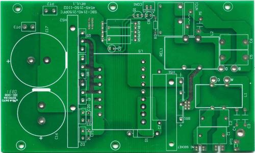
PCB screen printing is an important process in PCB production and also determines the quality of the finished PCB board. So, what are the specifications and requirements for PCB screen printing? 1. All components, installation holes, and positioning holes have corresponding silk screen markings. In order to facilitate the installation of the finished board, the installation holes on the PCB are marked with H1, H2,... Hn by screen printing. 2. Silk screen characters should follow the principle of going from left to right and from bottom to top as much as possible; For devices with polarity such as electrolytic capacitors and diodes, try to maintain consistent orientation within each functional unit. 3. There is no silk screen on the solder pads of the devices and the tin channels that need to be coated with tin, and the device tag number should not be obstructed by the devices after installation; The silk screen should not be pressed on the through hole or solder pad to avoid los
When high-speed PCB wiring is used, the signal will reflect in the transmission channel when the impedance does not match during transmission; The fundamental way to eliminate reflection is to make the impedance of the transmitted signal match well. So, what wiring rules should be followed for impedance matching of high-speed PCB signals? Due to the larger difference between the load impedance and the characteristic impedance of the transmission line, the greater the reflection, it is necessary to make the characteristic impedance of the signal transmission line equal to the load impedance as much as possible; At the same time, it is also important to note that there should be no sudden changes or corners in the transmission line on the PCB, and to try to maintain continuous impedance at each point of the transmission line, otherwise there will also be reflections between different sections of the transmission line. This requires that the following wiring rules must be followed wh
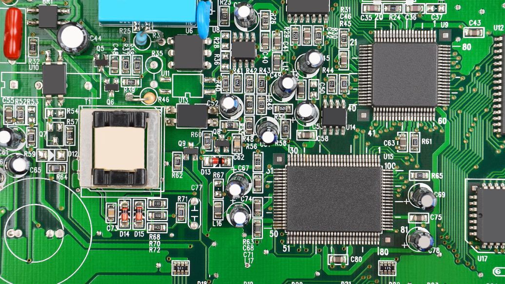
Circuit boards are known as the "mother of electronic components" and are essential basic accessories in electronic devices. Nowadays, there are many circuit board manufacturers on the market. With the development of circuit board production technology, many PCB buyers have gradually begun to understand the basic characteristics of Shenzhen circuit board manufacturers. So, what are the characteristics of excellent Shenzhen circuit board manufacturers? 1、 Having a strong R&D team The reason why Shenzhen circuit board manufacturers are able to produce high-quality circuit boards is that they have a professional research and development team that can provide plasticity suggestions for prototype products in the design stage. In addition, excellent core technical personnel from manufacturers have years of experience in circuit board research and development, which enables them to produce PCB circuit board products with quality assurance strictly in accordance with industry standards a
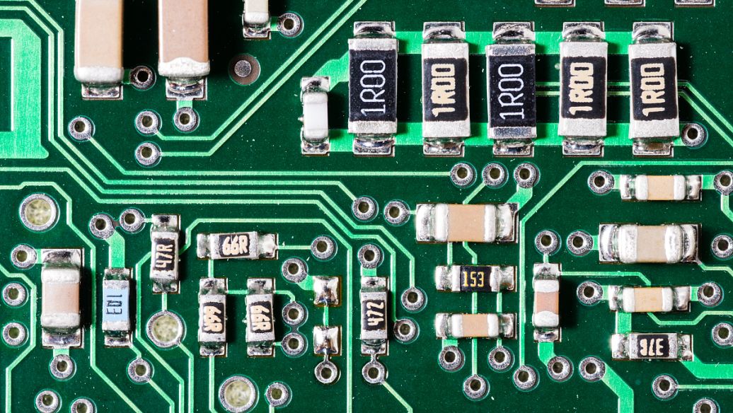
When customers customize PCB products, they always make more in case of unexpected needs. Over time, there may be the phenomenon of PCB boards expiring but being ignored by oneself. So, what are the hazards of using expired PCB circuit boards? 1. Expired PCB may cause oxidation of surface solder pads After oxidation of the solder pad, it will cause poor soldering, which may ultimately lead to functional failure or the risk of parts falling out. The antioxidant effect of different surface treatments on circuit boards may vary, and in principle, ENIG requires that they be used up within 12 months; OSP requires it to be used up within six months, and it is recommended to follow the shelf life of the PCB factory to ensure quality. 2. Expired PCB may absorb moisture and cause board explosion When the circuit board undergoes soldering after moisture absorption, it may cause problems such as popcorn effect, board explosion, or delamination. Although this problem can be solved through

Nowadays, the development of circuit boards is becoming more mature, and their technical level is constantly being updated. A PCB circuit board needs to go through various production processes from prototype to finished product. Sinking process is a commonly used surface treatment process in PCB circuit boards; Next, let the Shenzhen PCB factory take you to understand the process of circuit board gold deposition. The gold deposition process is to deposit a nickel gold coating with stable color, good brightness, flat coating, and good solderability on the surface of PCB printed circuits through chemical reactions; Because of weak adhesion, it is also known as soft gold. Because sinking gold is softer than plating gold, making gold fingers from sinking gold plates is not wear-resistant. The PCB board after sinking gold presents a golden yellow color, which is brighter and more beautiful than the color of gold plating. The Shenzhen PCB factory has summarized its characteristics as fo
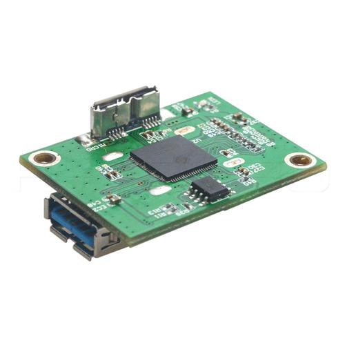
The problem of blackening of the electroplating gold layer often occurs, which affects the quality and performance of the circuit board. So, what are the reasons for the blackening of the electroplating gold layer on PCB board copying? 1. Thickness control of nickel plating layer PCB electroplating gold layer is generally very thin, reflected on the surface of electroplating gold, many of which are caused by poor performance of nickel electroplating. Generally, a thin nickel plating layer can cause the appearance of the product to turn white and black. Generally, it is necessary to electroplate the nickel layer thickness to around 5UM to be sufficient. 2. Condition of plating nickel cylinder solution If the nickel cylinder solution is not well maintained for a long time and carbon treatment is not carried out in a timely manner, the nickel layer electroplated will easily produce flaky crystals, increase the hardness and brittleness of the coating. Serious problems can result in b
Inquiry Now

