 +86 755 2794 4155
  sales@knownpcb.com
-
Shenzhen KNOWNPCB Technology Co., Ltd.
 +86 755 2794 4155
  sales@knownpcb.com
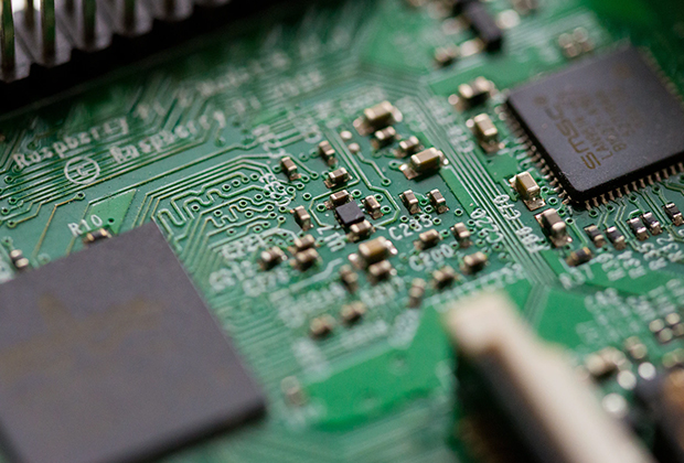
Have you noticed that now more and more of our lighting is using led lighting.What is LED? Compared to the traditional light bulbs, LEDs have lower power consumption, longer lifetime and higher energy efficiency. In the PCB industry,when we say LED PCB, it refers to the pcb used for LED lighting, if you are looking for a suitable LED PCB for your lighting system, this article may bring you something. WHAT ARE LEDS COMPOSED OF?LED is an initial light-emitting diode that produces light when an electric current passes through. LEDs typically have negative and positive electrodes, which generate light in the visible light region.The LEDS are glued to the PCB by soldering process and have electrical connections for lighting.Since light-emitting diodes dissipate a lot of heat when they are in use, when you are designing LED, the metal core is usually the best choice for LED PCB, it is because that it dissipates heat more faster. Among them, the metal material aluminum is the most widely used
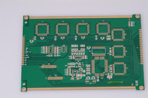
For two-layer boards, controlling EMI radiation is mainly considered from wiring and layout; The electromagnetic compatibility issues of single-layer and double-layer boards are becoming increasingly prominent. The main reason for this phenomenon is that the signal circuit area is too large, which not only generates strong electromagnetic radiation, but also makes the circuit sensitive to external interference. The simplest way to improve the electromagnetic compatibility of the circuit is to reduce the loop area of key signals; Key signals mainly refer to signals that generate strong radiation and signals that are sensitive to external boundaries. Single and double layer boards are typically used in low-frequency simulation designs below 10KHz: 1) Route the power supply in a radial pattern on the same layer and minimize the total length of the lines; 2) When using power and ground wires, approach each other closely; Lay a ground wire next to the critical signal line, which sho

The heat generated during the operation of electronic devices rapidly increases the internal temperature of the equipment. If this heat is not dissipated in a timely manner, the equipment will continue to heat up, and the reliability of electronic devices will decrease. Therefore, heat dissipation treatment for circuit boards is very important. So, what are the cooling methods for PCB circuit boards? 1. High heating device with heat sink and heat conduction plate. When there are a few components in the PCB that have a large heat output (less than 3), a heat sink or heat transfer tube can be added to the heating device; When the temperature cannot drop, a radiator with a fan can be used to enhance the heat dissipation effect. When there are a large number of heating devices (more than 3), a large heat dissipation cover (plate) can be used, and the heat dissipation cover can be buckled onto the surface of the components as a whole to dissipate heat in contact with each component. 2.
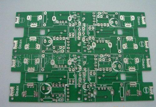
There is an old saying: PCB design involves 90% layout and 10% wiring. So, what are the skills for PCB wiring? 1. Don't rely on your automatic router Almost all PCB design software has a tool called an automatic router, but an automatic router will never replace itself in wiring and should only be used for a few reasons, including: Accurate. After placing all components, an automatic router can be used to view the completion level obtained. Bottleneck. You can also use an automatic router to discover bottlenecks and other critical connection points that may not be visible during component placement. Inspiration. You can use an automatic router as a source of inspiration to understand how to route some traces that you cannot complete. In addition to the above reasons, it is recommended not to rely on automatic wiring to complete all wiring on the layout of the circuit board. 2. Understand the manufacturer's specifications Before starting to lay copper wiring, please call or
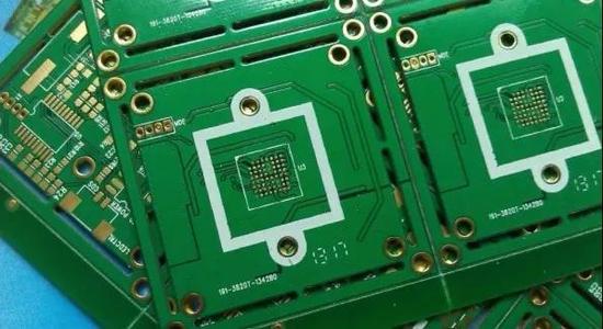
1. Parasitic capacitance The through-hole itself has parasitic capacitance to the ground. If the diameter of the isolation hole on the floor layer of the through-hole is known to be D2, the diameter of the through-hole pad is D1, the thickness of the PCB board is T, and the dielectric constant of the board substrate is ε, The parasitic capacitance of the via is approximately C=1.41 ε TD1/(D2-D1). The main impact of parasitic capacitance on the circuit caused by vias is that it prolongs the rise time of the signal and reduces the speed of the circuit. For example, for a PCB board with a thickness of 50Mil, if a through-hole with an inner diameter of 10Mil and a pad diameter of 20Mil is used, and the distance between the pad and the ground copper area is 32Mil, we can approximately calculate the parasitic capacitance of the through-hole using the above formula as follows: C=1.41 × four point four × zero point zero five zero × 0.020/(0.032-0.020)=0.517pF The variation in rise time
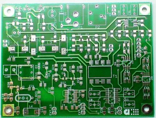
Through holes (via) are an important component of PCB circuit boards, and the cost of drilling holes usually accounts for 30% to 40% of PCB manufacturing costs. Simply put, every hole on a PCB can be referred to as a through hole. So, what are the classification and composition of through-holes on PCB circuit boards? 1、 Classification of vias From the perspective of function, vias can be divided into two categories: one is used as electrical connections between layers; The second is used for fixing or positioning components. From a process perspective, through holes can be further divided into three categories: blind holes, buried holes, and through holes. Blind holes are located on the top and bottom surfaces of circuit boards, with a certain depth, used for connecting surface and inner circuits. The depth of the holes usually does not exceed a certain ratio (aperture). The buried hole is a connecting hole located on the inner layer of the circuit board, and it will not extend
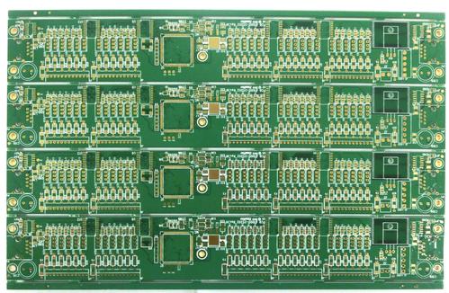
High frequency board refers to a special type of circuit board with high electromagnetic frequency, used for PCBs in the fields of high frequency (frequency greater than 300MHz or wavelength less than 1 meter) and microwave (frequency greater than 3GHz or wavelength less than 0.1 meter). It is a circuit board produced on a microwave substrate copper clad board using partial processes of ordinary rigid circuit board manufacturing methods or special processing methods. Generally speaking, high-frequency boards can be defined as circuit boards with frequencies above 1GHz. So, what are the main factors to consider when choosing a suitable high-frequency PCB board? Let the editor decrypt it for you: 1. Manufacturability; For example, how about the multiple pressing performance, temperature performance, CAF/heat resistance, mechanical toughness (good reliability), and fire resistance level; 2. Various performance matching with the product (electrical, performance stability, etc.); Lo
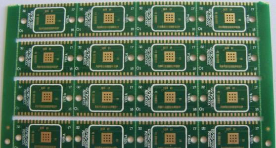
1、 Contact the manufacturer Firstly, it is necessary to inform the manufacturer of the documents, process requirements, and quantity. Regarding "What parameters do you need to provide for PCB circuit board sampling to the manufacturer?" You can click on this article to learn and provide the necessary information. Then, professionals will provide you with quotations, place orders, and follow up on the production progress. 2、 Material cutting Purpose: According to the requirements of the engineering data MI, cut into small production pieces on large sheets that meet the requirements, and produce small pieces that meet the customer's requirements. Process: Large plate material → Cutting according to MI requirements → Curing plate → Fillet angle/edge grinding → Plate discharge 3、 Drilling Purpose: Based on engineering data, drill the required hole diameter at the corresponding position on the sheet material that meets the required size. Process: Stacking pin → Upper plate → Dril

Welding is an important process in PCB circuit board sampling. We often encounter many welding defects when making PCBs. So, what are the common welding defects of PCB circuit boards? 1. False soldering: There is a clear black boundary between solder and component leads or copper foil, and solder is concave towards the boundary. Hazard: The circuit board cannot function properly. Reason: 1) Component leads are not cleaned properly, not tin plated or oxidized; 2) The printed board was not cleaned properly and the quality of the soldering flux sprayed was poor. 2. Solder accumulation: The solder joint structure is loose, white, and dull. Hazard: Insufficient mechanical strength, possible false soldering. Reason: 1) Poor solder quality; 2) Insufficient welding temperature; 3) Loose component leads. 3. Excessive solder: The solder surface is convex. Hazard: Waste solder and may contain defects. Reason: The solder was evacuated too late. 4. Insufficient solder: The welding are
Inquiry Now

