 +86 755 2794 4155
  sales@knownpcb.com
-
Shenzhen KNOWNPCB Technology Co., Ltd.
 +86 755 2794 4155
  sales@knownpcb.com
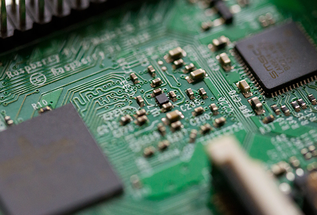
Have you noticed that now more and more of our lighting is using led lighting.What is LED? Compared to the traditional light bulbs, LEDs have lower power consumption, longer lifetime and higher energy efficiency. In the PCB industry,when we say LED PCB, it refers to the pcb used for LED lighting, if you are looking for a suitable LED PCB for your lighting system, this article may bring you something. WHAT ARE LEDS COMPOSED OF?LED is an initial light-emitting diode that produces light when an electric current passes through. LEDs typically have negative and positive electrodes, which generate light in the visible light region.The LEDS are glued to the PCB by soldering process and have electrical connections for lighting.Since light-emitting diodes dissipate a lot of heat when they are in use, when you are designing LED, the metal core is usually the best choice for LED PCB, it is because that it dissipates heat more faster. Among them, the metal material aluminum is the most widely used
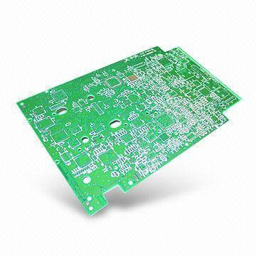
PCBA, which refers to the assembly, mounting, and welding of PCB components, is the core process in PCBA. So, what are the precautions for PCB processing by Shenzhen circuit board manufacturers? 1、 Transportation: To prevent damage to PCBA, during transportation, it is necessary to: 1. Container: Anti static turnover box. 2. Isolation material: anti-static pearl cotton. 3. Placement spacing: There is a distance greater than 10mm between boards and between boards and boxes. 4. Placement height: There is a space greater than 50mm from the top surface of the turnover box. 2、 PCBA processing and washing requirements: 1. Board surface requirements: Clean, with no stains on Wuxi beads and component pins. 2. Devices that should be protected during board washing: wires, connecting terminals, relays, switches, polyester capacitors, and other devices. 3、 Component requirements: All components must not exceed the edge of the PCB board after installation. 4、 Welding requirements: 1.

Printed circuit boards (PCBs) are an indispensable part of electronic devices, and their performance and reliability directly affect the operation of the entire system. PCB (Printed Circuit Board), also known as Printed Circuit Board (PCB) in Chinese, is an important electronic component that supports electronic components and serves as a carrier for the electrical interconnection of electronic components. Due to its use of electronic printing technology, it is called a "printed" circuit board. Cabling is a key step in PCB design, which determines the performance and stability of the circuit board. This article will explore the wiring principles and practical techniques of PCB boards to help engineers achieve better results in design. Wiring principles Following the circuit schematic diagram Wiring should strictly follow the circuit schematic to ensure correct wiring connections and prevent short or open circuit problems. During the wiring process, each component in the circuit
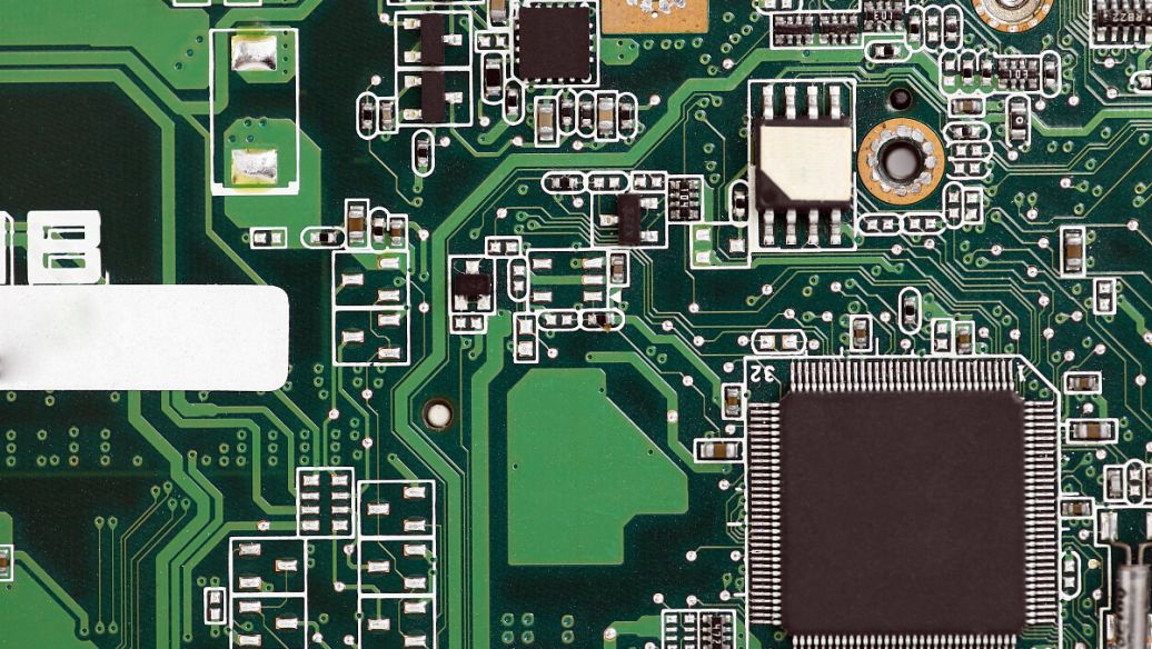
During the production process of PCB circuit boards, due to the inability of printed solder paste and solderless PCB assembly boards to fix the test end of thermocouples, it is necessary to use the actual welded product for temperature testing. So, how to conduct PCB board temperature limit testing? 1、 Select test points: Based on the complexity of the PCB assembly board and the number of channels in the collector, select at least three representative temperature test points that can reflect the high, medium, and low temperatures on the PCB surface assembly board. 2、 Fixed thermocouple: Use high-temperature solder to weld the test ends of multiple thermocouples onto the test points (solder joints), and the solder on the original solder joints must be cleaned before welding; Alternatively, use high-temperature adhesive tape to attach the test ends of the thermocouples to each temperature test point on the PCB. 3、 Insert the other end of the thermocouple into the machine table at
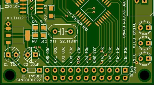
PCBA, which refers to the assembly, mounting, and welding of PCB components, is the core process in PCBA. So, what are the precautions for PCB processing by Shenzhen circuit board manufacturers? 1、 Transportation: To prevent damage to PCBA, during transportation, it is necessary to: 1. Container: Anti static turnover box. 2. Isolation material: anti-static pearl cotton. 3. Placement spacing: There is a distance greater than 10mm between boards and between boards and boxes. 4. Placement height: There is a space greater than 50mm from the top surface of the turnover box. 2、 PCBA processing and washing requirements: 1. Board surface requirements: Clean, with no stains on Wuxi beads and component pins. 2. Devices that should be protected during board washing: wires, connecting terminals, relays, switches, polyester capacitors, and other devices. 3、 Component requirements: All components must not exceed the edge of the PCB board after installation. 4、 Welding requirements: 1.
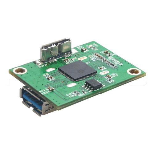
Printed circuit boards (PCBs) are an indispensable part of electronic devices, and their performance and reliability directly affect the operation of the entire system. PCB (Printed Circuit Board), also known as Printed Circuit Board (PCB) in Chinese, is an important electronic component that supports electronic components and serves as a carrier for the electrical interconnection of electronic components. Due to its use of electronic printing technology, it is called a "printed" circuit board. Cabling is a key step in PCB design, which determines the performance and stability of the circuit board. This article will explore the wiring principles and practical techniques of PCB boards to help engineers achieve better results in design. Wiring principles Following the circuit schematic diagram Wiring should strictly follow the circuit schematic to ensure correct wiring connections and prevent short or open circuit problems. During the wiring process, each component in the circuit
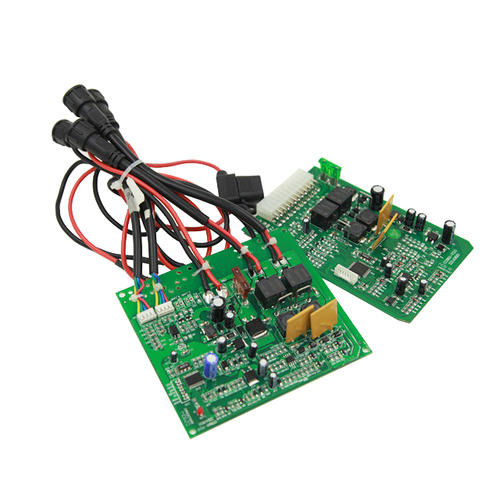
During the production process of PCB circuit boards, due to the inability of printed solder paste and solderless PCB assembly boards to fix the test end of thermocouples, it is necessary to use the actual welded product for temperature testing. So, how to conduct PCB board temperature limit testing? 1、 Select test points: Based on the complexity of the PCB assembly board and the number of channels in the collector, select at least three representative temperature test points that can reflect the high, medium, and low temperatures on the PCB surface assembly board. 2、 Fixed thermocouple: Use high-temperature solder to weld the test ends of multiple thermocouples onto the test points (solder joints), and the solder on the original solder joints must be cleaned before welding; Alternatively, use high-temperature adhesive tape to attach the test ends of the thermocouples to each temperature test point on the PCB. 3、 Insert the other end of the thermocouple into the machine table at
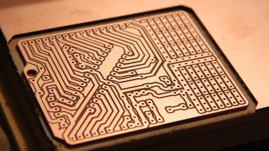
The problem of blackening of the electroplating gold layer often occurs, which affects the quality and performance of the circuit board. So, what are the reasons for the blackening of the electroplating gold layer on PCB board copying? 1. Thickness control of nickel plating layer PCB electroplating gold layer is generally very thin, reflected on the surface of electroplating gold, many of which are caused by poor performance of nickel electroplating. Generally, a thin nickel plating layer can cause the appearance of the product to turn white and black. Generally, it is necessary to electroplate the nickel layer thickness to around 5UM to be sufficient. 2. Condition of plating nickel cylinder solution If the nickel cylinder solution is not well maintained for a long time and carbon treatment is not carried out in a timely manner, the nickel layer electroplated will easily produce flaky crystals, increase the hardness and brittleness of the coating. Serious problems can result in
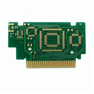
The PCB circuit board is only a complete device after processing, and can be used in applied electronic products. The PCBA process is the combination of SMT processing and DIP processing. Today, the editor will share with you what processes are included in the processing of PCB by Shenzhen circuit board manufacturers. 1、 Single sided DIP insertion PCB boards that require plugins can be welded and fixed by workers after inserting electronic components, followed by wave soldering, cutting and washing the board. 2、 Single sided SMT mounting Add solder paste to the component pad, and after the solder paste printing is completed, the relevant electronic components are reflow soldered and then reflow soldered. 3、 Single sided mixed packaging PCB boards are printed with solder paste, installed with electronic components and fixed by reflow soldering. After quality inspection is completed, DIP insertion is performed, followed by wave soldering or manual soldering. 4、 Double sided SM
Inquiry Now

