


2008Founded in 2008

5000+5000 Models/Month

100000+More than 100000sqm

150000+150000sqm /month

4000+Serving 4,000+ Valued Customers Worldwide
From PCB fabrication to PCBA, KnownPCB helps teams move faster with engineering review, quick-turn manufacturing, and reliable production support with proven yield and on-time delivery. We act as a reliable manufacturing partner for engineering teams, offering specialized support for advanced board structures such as 2-n-2 HDI, heavy copper, and metal core PCBs.

HDI PCBHDI interconnect design supports via-in-pad and dense BGA routing applications

Metal Core PCBHigh voltage, Vibration resistance, Long lifecycle
ENIG PCBENIG PCB Solution and Manufacturing

Heavy Copper PCBHigh-current capability with stable thermal performance

High-Frequency & High-Speed PCBLow-loss transmission for high-speed signals

Multilayer PCBHigh-density circuits with signal integrity

Flexible PCB(FPC)Fast Turn Flex PCB ( Prototype & Fabrication) for complex electronics and wearable products

Rigid-Flex PCBUltra-thin circuits for dynamic bending use
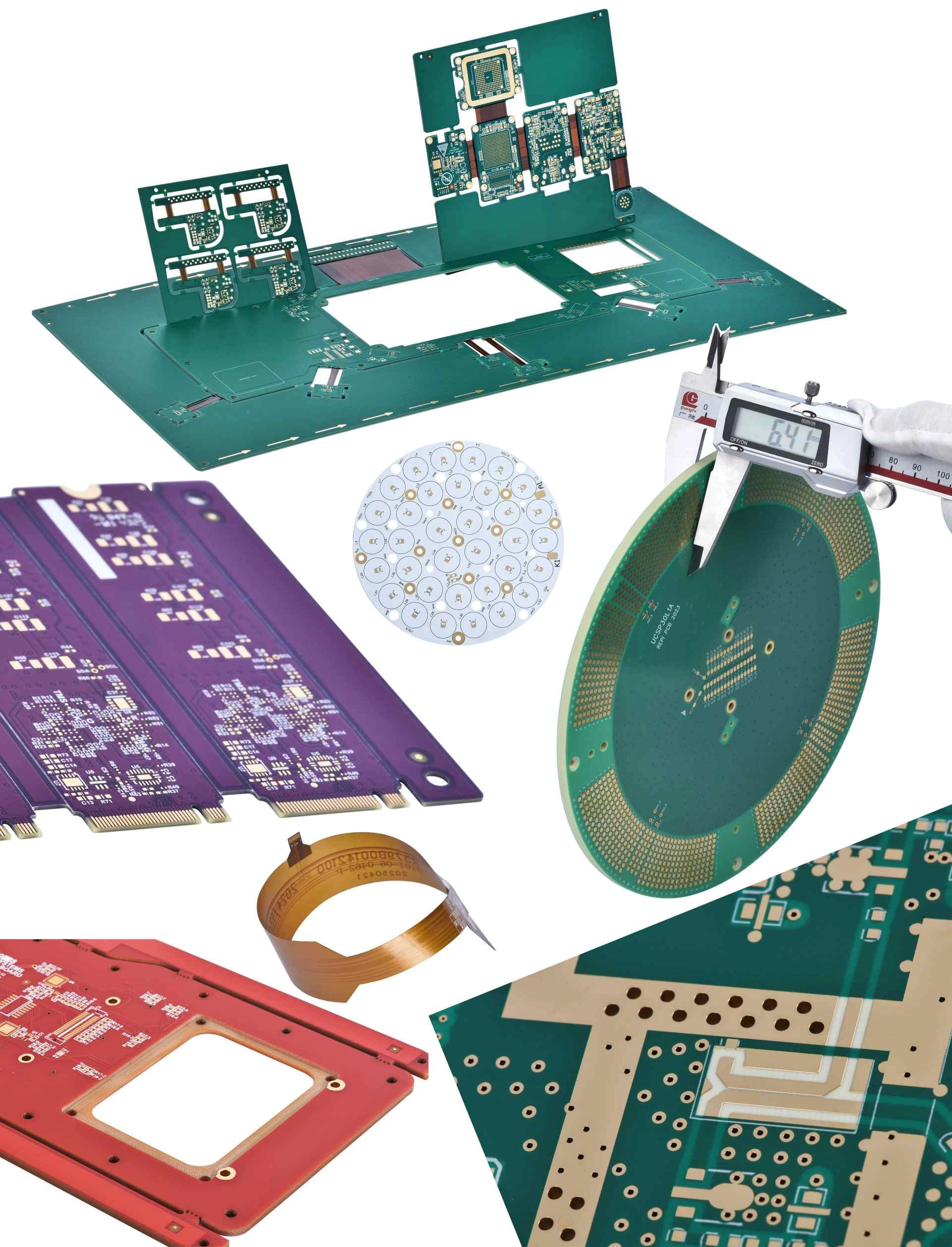

Master complex PCB builds with expert High-Mix Low-Volume manufacturing solutions. | Shenzhen PCB Fabrication

From prototypes to production: Seamless, high-precision turnkey PCB assembly solutions

KnownPCB Testing Methods: Maximize product reliability with professional, system-level PCB functional testing.

Robust PCB quality management ensures reliable performance and strict industry compliance.
KnownPCB focuses on PCB prototyping and low-volume manufacturing for challengeable PCB projects, including 3-stage HDI and heavy copper PCBs. The manufacturing capabilities extend to key applications related to power management, signal transmission, and drive system in automotive, industrial, medical, communications etc.
From quick-turn PCB prototypes to low-volume pilot runs, we have served more than 4,000 customers worldwide. Explore KnownPCB’s product capabilities, engineering support, quality assurance, and application solutions.
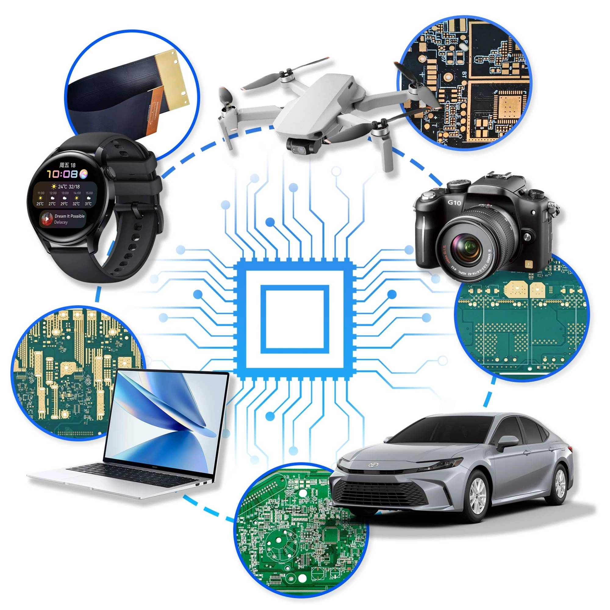
Across every industry, KNOWNPCB helps bring product ideas to life by solving real PCB challenges. From high-density design to heat management and performance stability, the team works side by side with customers—from early prototyping to volume launch—to create products that truly succeed in the market.
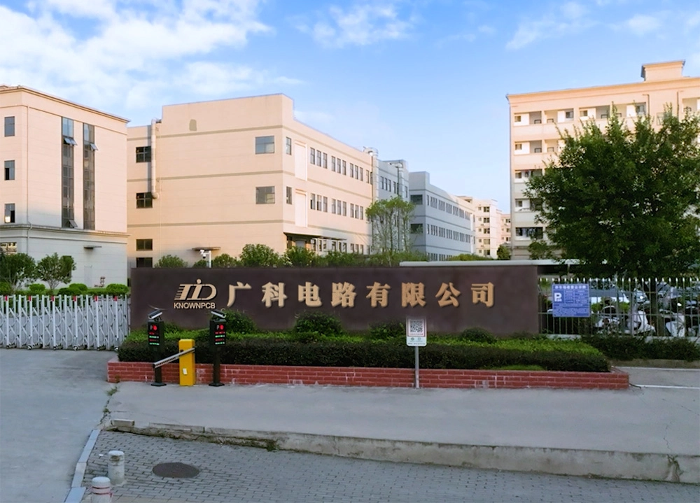
At KNOWNPCB, “Get More by Less” means helping you achieve greater performance with less effort, time, and risk. Since 2008, we’ve built an engineering-driven approach that simplifies your PCB journey — from DFM support and quick-turn prototypes to reliable volume production. All of which, powered by state-of-the-art equipment and rigorous quality management, KNOWNPB has earned the trust of 4,000+ global customers who value consistency, transparency, and results.

An EV inverter gate driver PCB can sit beside a power module and still have a long electrical gate loop. The outgoing gate trace may be short, while the return travels through a connector, a shared source conductor, or a distant plane connection. The complete outgoing-and-return path determines th...
A BMS schematic can separate the current-sense signal from the load current, yet the PCB footprint can join them again. A copper pour touching the sense pickup includes part of the power path in the measurement. A later layout revision may introduce that connection without changing the schematic n...
A laminate datasheet says “breakdown voltage.” The lighting specification says “working voltage.” The purchase order asks for “high voltage aluminum PCB.” These statements do not define the same requirement. An LED aluminum PCB dielectric must be selected against the electrical stress and insulati...
Operations Center Shenzhen KnownPCB Technology Co.,LtdBldg D,Liantangkeng Industrial Area,Qianjin Road,Xixiang Street,Bao'an Dist.,Shenzhen City,Guangdong Province,518102,China.
| Have Question? Request a call back |
 Consumer & IoT Electronics
 Energy & Power Electronics
 Automotive & EV Systems
 Telecom 5G & High-Speed Computing
 Industrial & Automation
 Medical & Healthcare Devices
 Aerospace, Defense & Avionics


