 +86 755 2794 4155
  sales@knownpcb.com
-
Shenzhen KNOWNPCB Technology Co., Ltd.
 +86 755 2794 4155
  sales@knownpcb.com
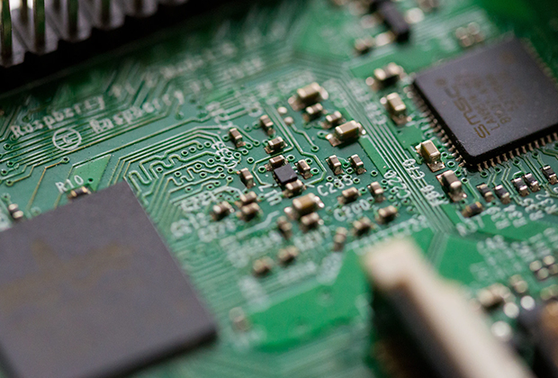
Have you noticed that now more and more of our lighting is using led lighting.What is LED? Compared to the traditional light bulbs, LEDs have lower power consumption, longer lifetime and higher energy efficiency. In the PCB industry,when we say LED PCB, it refers to the pcb used for LED lighting, if you are looking for a suitable LED PCB for your lighting system, this article may bring you something. WHAT ARE LEDS COMPOSED OF?LED is an initial light-emitting diode that produces light when an electric current passes through. LEDs typically have negative and positive electrodes, which generate light in the visible light region.The LEDS are glued to the PCB by soldering process and have electrical connections for lighting.Since light-emitting diodes dissipate a lot of heat when they are in use, when you are designing LED, the metal core is usually the best choice for LED PCB, it is because that it dissipates heat more faster. Among them, the metal material aluminum is the most widely used
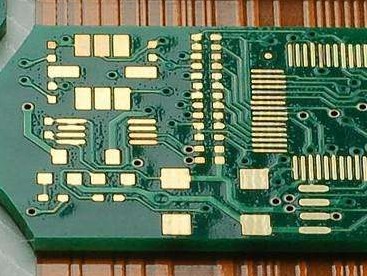
Many special components are often used in PCB layout, and if the layout is not handled properly, it will directly affect the performance and quality of the PCB circuit board. So, what are the layout requirements for special components on PCB circuit boards? 1. Layout requirements for crimping devices (1) There should be no components greater than 3mm around the crimping device surface, and no welding components should be present around 1.5mm; There must be no components within a distance of 2.5mm from the center of the pin hole of the crimping device on the opposite side of the crimping device. (2) There should be no components within 1mm around the crimping device. 2. Layout requirements for thermal sensitive devices (1) Thermal sensitive devices (such as electrolytic capacitors, crystal oscillators, etc.) should be kept away from high thermal devices as much as possible. (2) The thermal sensitive device should be tightly attached to the tested component and away from the hi
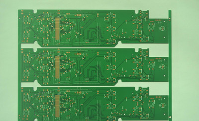
PCB circuit boards can be divided into single-sided, double-sided, and multi-layer. Multilayer boards refer to circuit boards with more than 4 layers, and currently there are over 100 layers of PCBs. Why are PCB multilayer boards even numbered? 1. Relatively speaking, even layer PCBs do have more advantages than odd layer PCBs. Due to the lack of a layer of medium and foil, the raw material cost of odd layer PCBs is slightly lower than that of even layer PCBs, but its processing cost is significantly higher than that of even layer PCBs. Odd layer PCBs require the addition of non-standard laminated core bonding processes on top of the core structure process. Before lamination bonding, the outer core requires additional processing, which increases the risk of scratches and etching errors on the outer layer. 2. Odd layer circuit boards are prone to bending. When the PCB cools down after the multi-layer circuit bonding process, different lamination tensions can cause the PCB to bend.
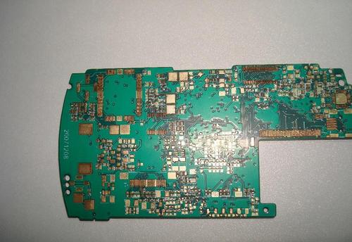
The question that many newcomers ask the most is: why are the vast majority of PCB board colors green? Today, the PCB engineer will come to answer this question for you. 1. Green ink is currently the most widely used and long-lasting ink, and it is also the cheapest in the market. Therefore, green is widely used as the main color for PCB products by many manufacturers. 2. Usually, during the production of PCB circuit boards, there are several processes that must go through the yellow light chamber, because green has a better effect in the yellow light chamber than other colors. In addition, when soldering components in SMT, PCB circuit board production needs to go through solder paste and lamination, as well as the final AOI calibration process. Optical positioning calibration is required, and boards with a green background color have better recognition effect on the instrument. 3. The production of PCB circuit boards may not necessarily be green, it depends on the color that the
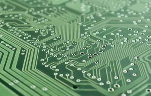
Many customers often ask: What are the common problems encountered in PCB circuit board design? Let professional PCB manufacturers tell you below. 1. Why do we try not to split across power sources when wiring? Because the signal spans different power layers, its return path becomes longer and more susceptible to interference. Of course, low-speed signals are acceptable, but high-speed signals should be carefully checked and avoided crossing as much as possible. 2. Some boards may have external input and output interfaces, and if their grounding design is not good, it can also affect normal operation and become a source of external electromagnetic interference, sending out the noise inside the board. Generally speaking, a separate interface ground will be separated and connected to the signal ground through thin wiring, which can be connected in series with a resistance of 0 ohms or a small resistance value. Common grounding symbols: PE, PGND, FG - protective grounding or casin
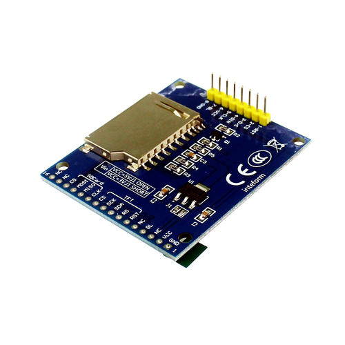
PCB layout and design have a significant impact on the way a circuit works, therefore, if printed circuit boards are designed in an effective manner, the circuit will work more reliably within its specification range. So, what are the issues to pay attention to in the layout and design of PCB circuit boards? 1. PCB design equipment For commercial development programs, CAD and computer-aided design packages may be required due to complexity. The functionality of PCB software varies greatly. Budget and even free software provide basic functions, while high-end software packages allow for more features to be included in the design. Simulation, complex routing, and more features are available. 2. Circuit schematic capture The first step in PCB design is to capture the circuit schematic. The circuit can be input into the schematic capture tool and can also be simulated during this stage. For applications such as RF circuit design, circuit simulation can lead to more optimization of

PCB design is an important step before PCB production. If not designed well, it will directly affect the performance and quality of the circuit board, causing the entire circuit board to be scrapped; Layout of components is an important aspect of PCB design. So, what are the requirements for PCB design and layout of components? 1. Aesthetics When designing a PCB, it is not only important to consider the orderly placement of components, but also to consider the graceful and smooth wiring. 2. Force The circuit board should be able to withstand various external forces and vibrations during installation and operation: it should have a reasonable shape, and the positions of various holes on the board should be arranged reasonably; Generally, the distance between the hole and the board edge should be at least greater than the diameter of the hole; It should also be noted that the weakest section of the plate caused by irregular holes should also have sufficient bending strength. 3.
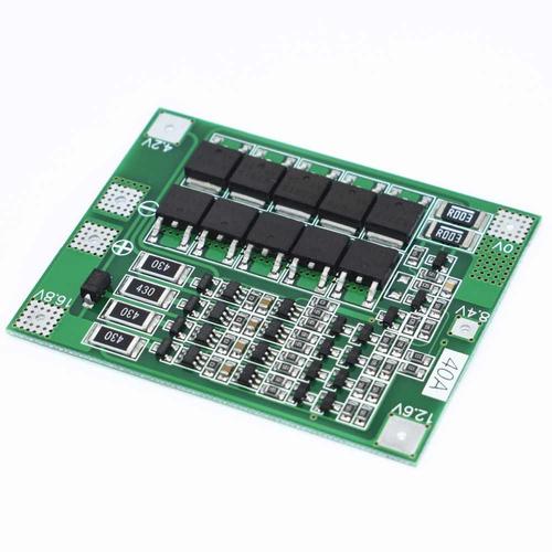
Rigid flexible combination board is a method of laminating a flexible circuit substrate and a rigid circuit substrate together, which has both the rigidity of a hard board and the flexibility of a soft board. So, what issues should be paid attention to when making rigid flexible composite boards? 1. The design of rigid flexible composite plates usually changes from rigidity to flexibility, and then to rigidity. The rigid region generally has more layers than the flexible region, and the material is transferred from FR-4 to polyimide in the transition region. When intersection occurs, the overlap between rigid and flexible materials needs to keep the holes away from the transition area to maintain integrity. In addition, many rigid and flexible designs incorporate reinforcing materials such as stainless steel or aluminum to provide additional support for connectors and components. 2. Flexible circuits have bent wires that can affect wiring. Due to possible material stress, it is n

Introduce the relevant content and situation of printed circuit boards to help everyone improve their understanding. Let's read the following content together with the editor. Printed circuit boards (PCBs) are convenient thin sheets used to accommodate interconnected electrical components in a simple, convenient, and economical manner. They are used as physical supports for installing and connecting different electrical components. The PCB is made of glass fiber, composite epoxy resin or any other composite material, and has a metal coated surface. They have etching made of metals and acids to create circuits through different integrated circuits (ICs) and other components on circuit boards. Solder connects ICs and other components to the surface of the circuit board. The copper tracks in the circuit board reduce the possibility of short circuits, misalignment, or misaligned wires. In this way, all components are firmly fixed to the circuit board without the need for complex wir
Inquiry Now

