 +86 755 2794 4155
  sales@knownpcb.com
-
Shenzhen KNOWNPCB Technology Co., Ltd.
 +86 755 2794 4155
  sales@knownpcb.com
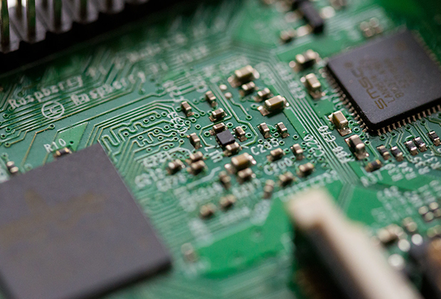
Have you noticed that now more and more of our lighting is using led lighting.What is LED? Compared to the traditional light bulbs, LEDs have lower power consumption, longer lifetime and higher energy efficiency. In the PCB industry,when we say LED PCB, it refers to the pcb used for LED lighting, if you are looking for a suitable LED PCB for your lighting system, this article may bring you something. WHAT ARE LEDS COMPOSED OF?LED is an initial light-emitting diode that produces light when an electric current passes through. LEDs typically have negative and positive electrodes, which generate light in the visible light region.The LEDS are glued to the PCB by soldering process and have electrical connections for lighting.Since light-emitting diodes dissipate a lot of heat when they are in use, when you are designing LED, the metal core is usually the best choice for LED PCB, it is because that it dissipates heat more faster. Among them, the metal material aluminum is the most widely used
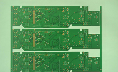
What problems will you encounter when designing circuit board samples? The following is a summary of ten common problems encountered in PCB sample design. 1、 Overlap of pads Overlapping solder pads means overlapping holes. During the drilling process, multiple drilling at one location can cause damage to the holes and result in scrapping. 2、 Graphic layer abuse Specific performance: Some useless connections were made on some graphics layers, and originally a four layer board was designed with circuits above five layers, which caused misunderstandings; Violation of conventional design, such as component surface design at the Bottom layer and welding surface design at the Top, causing inconvenience, etc. Therefore, maintaining the integrity and clarity of the graphic layer during design. 3、 Character shuffling Specifically, the character cover solder pad SMD solder pad brings inconvenience to the on/off testing of circuit boards and the welding of components; Also, the characte
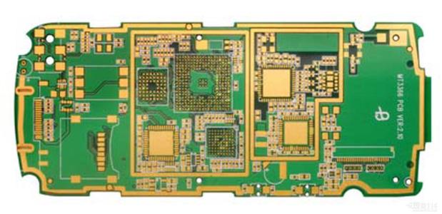
Aluminum substrate is a metal based copper clad plate with good heat dissipation function, commonly used for making LED lights. Let's now understand the difficulties and production specifications of the aluminum substrate production process. 1. Aluminum substrates are often used in power devices with high power density, so copper foil is relatively thick. If copper foil above 3oz is used, the etching process requires engineering design line width compensation. 2. The aluminum substrate surface of the aluminum substrate is protected with a protective film in advance during PCB processing, otherwise some chemicals may corrode the aluminum substrate surface and cause appearance damage. 3. The milling cutter used in the production of fiberglass board has a relatively low hardness and fast milling speed; The milling cutters used in the production of aluminum substrates have high hardness, and the milling cutter speed is at least two-thirds slower. 4. To produce fiberglass panels, on
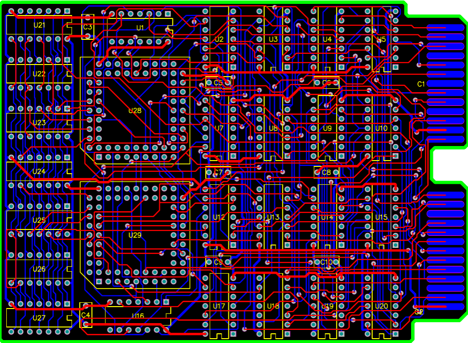
l. Areas with unreasonable design are most prone to malfunctions What are the unreasonable design aspects of industrial circuit boards? Firstly, there is a heat dissipation issue, as many circuit boards are damaged due to poor heat dissipation design; Secondly, the copper foil wire of the printed circuit board is used. The copper foil of the power supply wire of the circuit board with poor quality is very thin, which is easily burnt off due to overcurrent, making the motherboard unable to work. 2. Frequently used areas are prone to malfunctions For example, the drive motor of industrial circuit boards, rotating shafts, switch tubes of switching power supplies, commonly used buttons on operation panels, etc. 3. Components with heavy loads, high power, and high operating voltage are most likely to malfunction The power supply, drive circuit, power control device, operational amplifier, etc. of industrial circuit boards are the most vulnerable to damage. These components are gene
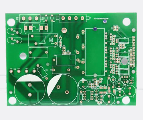
In PCB design, wiring is an important step in completing product design, and it can be said that the previous preparation work was done for it. PCB wiring includes single-sided wiring, double-sided wiring, and multi-layer wiring. There are also two types of wiring methods: automatic wiring and interactive wiring. Today, let professional engineers explain in detail what PCB wiring rules and techniques are available for you? 1. Handling of power and ground wires The interference caused by improper handling of power and ground wires can lead to a decrease in product performance, and sometimes even affect the success rate of the product. Therefore, the wiring of power and ground wires should be taken seriously, and the noise interference generated by the power and ground wires should be minimized to ensure the quality of the product. The specific approach is as follows: (1) Add a coupling capacitor between the power supply and ground wire. (2) Try to widen the width of the power a
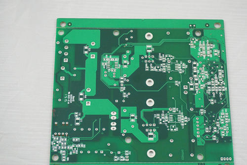
Copper deposition is the abbreviation for chemical copper plating, also known as through hole plating, abbreviated as PTH. It refers to the chemical deposition of a thin layer of chemical copper on a non conductive hole wall substrate that has been drilled, to serve as the substrate for subsequent copper plating. So, what are the processes for copper deposition on PCB circuit boards? Let's take a look together with the editor: 1、 Decomposition of PTH process: Alkaline degreasing → Second or third stage countercurrent rinsing → Coarsening (micro etching) → Second stage countercurrent rinsing → Pre leaching → Activation → Second stage countercurrent rinsing → Gelation → Second stage countercurrent rinsing → Copper precipitation → Second stage countercurrent rinsing → Acid leaching. 2、 Detailed process explanation of PTH: 1. Alkaline degreasing: Remove oil stains, fingerprints, oxides, and dust inside the holes on the board surface; Adjust the pore wall from negative charge to pos
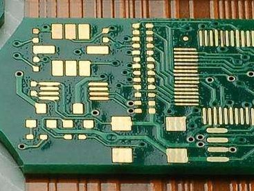
Filtering technology is an effective measure to suppress interference, especially in dealing with conducted interference and certain radiated interference of EMI signals in switching power supplies, which has obvious effects. So, what issues should we pay attention to regarding PCB circuit board filtering technology? 1. Differential mode interference and common mode interference Any conducted interference signal on the power line can be represented by differential and common mode interference signals. In general, the amplitude of differential mode interference is small, the frequency is low, and the interference caused is relatively small; Common mode interference has a large amplitude and high frequency, and can also generate radiation through wires, resulting in significant interference. Therefore, in order to weaken conducted interference, the EMI signal should be controlled below the limit level specified in relevant EMC standards. In addition to suppressing interference sou
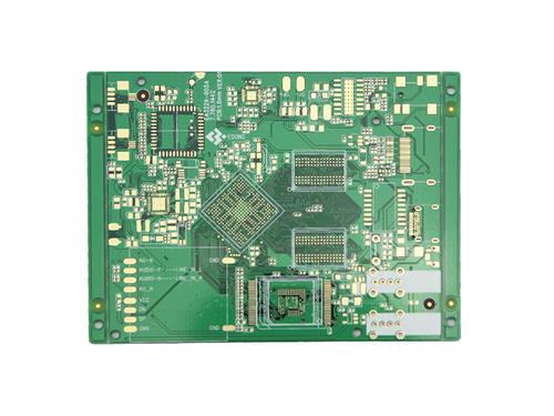
Firstly, distinguish the quality of FPC circuit boards from their appearance: 1. Standards for size and thickness. Customers can measure and check whether the product meets the thickness and specifications specified in the production drawings. 2. Light and color. Circuit boards are all covered with ink. If the color of the board is not bright and there is less ink, it indicates that the quality of the board itself is not good. 3. Weld appearance. Due to the large number of parts on the circuit board, poor welding can lead to parts falling off easily. Careful identification can provide a preliminary assessment of quality. Secondly, high-quality FPC circuit boards have the following requirements: 1. It is required that the components be easy to use after installation, that is, the electrical connection should meet the requirements; 2. The line width, thickness, and distance of the line meet the requirements to avoid heating, open circuit, and short circuit of the line; 3. T
1. SIG GND (PWR) - PWR (GND) - SIG; 2. GND SIG (PWR) - SIG (PWR) - GND; The potential issue with the above two stacked designs is the traditional 1.6mm (62mil) plate thickness. The interlayer spacing will become large, which is not conducive to controlling impedance, interlayer coupling, and shielding; Especially, the large spacing between the power layers reduces the board capacitance, which is not conducive to filtering out noise. The first solution is usually applied in situations where there are many chips on the board. This solution can achieve good SI performance, but it is not very good for EMI performance. It mainly needs to be controlled through wiring and other details. The second solution is usually applied in situations where the chip density on the board is low enough and there is sufficient area around the chip. In this scheme, the outer layer of the PCB is a layer, and the middle two layers are both signal/power layers. From the perspective of EMI control, This
Inquiry Now

