 +86 755 2794 4155
  sales@knownpcb.com
-
Shenzhen KNOWNPCB Technology Co., Ltd.
 +86 755 2794 4155
  sales@knownpcb.com
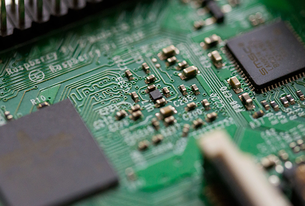
Have you noticed that now more and more of our lighting is using led lighting.What is LED? Compared to the traditional light bulbs, LEDs have lower power consumption, longer lifetime and higher energy efficiency. In the PCB industry,when we say LED PCB, it refers to the pcb used for LED lighting, if you are looking for a suitable LED PCB for your lighting system, this article may bring you something. WHAT ARE LEDS COMPOSED OF?LED is an initial light-emitting diode that produces light when an electric current passes through. LEDs typically have negative and positive electrodes, which generate light in the visible light region.The LEDS are glued to the PCB by soldering process and have electrical connections for lighting.Since light-emitting diodes dissipate a lot of heat when they are in use, when you are designing LED, the metal core is usually the best choice for LED PCB, it is because that it dissipates heat more faster. Among them, the metal material aluminum is the most widely used
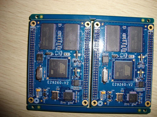
The short circuit fault of the module half hole PCB board is one of the common problems that immediately cause the module half hole PCB board to not work. There are many reasons for this type of problem, and everyone will analyze it one by one below. 1) The main reason for PCB short circuit faults is the poor design of the solder pad. In this case, it is possible to change the circular solder pad to an elliptical shape, increase the spacing between points, and avoid short circuit faults. 2) Inappropriate design solutions for PCB component orientation can also lead to short circuit faults on wooden boards and prevent them from working properly. If the foot of a SOIC is parallel to the tin wave, it is very easy to cause a short circuit fault accident. At this time, the orientation of the part can be adjusted appropriately to make it perpendicular to the tin wave. 3) There is also a probability that it can lead to a common fault of PCB short circuit, which is fully automatic softwa
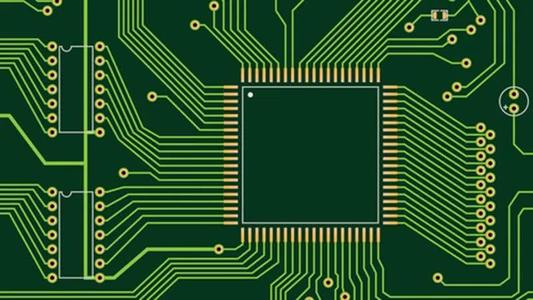
Why do module half hole PCB boards require vacuum packaging bags? Although this issue is small, it is indeed a problem that many circuit board manufacturers attach great importance to. Due to the lack of good sealing performance of the module half hole PCB board, its surface gold deposition, tin spraying, and welding layer positions will be oxidized by air, which poses a threat to welding and is not conducive to production and manufacturing. So, how do you store the module half hole PCB board? A circuit board is not like any other product, it cannot touch gas or water. The module half hole PCB vacuum pump cannot be damaged. When loading, a layer of bubble pad should be placed next to the small box. The bubble pad has good water absorption ability, which has a very good effect on waterproofing. Naturally, waterproof beads are also indispensable. Then classify and label the pollutants. After packing, the small box must be separated from the wall, stored off the ground in a dry and c

The quality and production efficiency of SMT chip placement processing are crucial for PCB circuit boards. If they are the foundation of PCB circuit boards, then SMT process materials are the bricks and stones of PCB circuit boards, playing a crucial role. Therefore, when designing the SMT process and resumes the production line, it is necessary to select appropriate process materials based on the process flow and requirements. SMT process materials include welding and SMT materials such as solder, solder paste, and adhesive, as well as process materials such as flux, cleaning agent, and heat conversion medium. Next, let's introduce the main functions of assembly process materials. (1) Solder and solder paste Solder is an important structural material in surface assembly processes. Different types of solder are used in different applications to connect the metal surface of the welded object and form solder joints. Reflow soldering uses solder paste, which is a welding material an
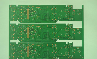
The SMT installation rate is very important for PCB companies. It can be said that many people are concerned about the SMT installation rate because it not only affects the processing cost of the production line, but also affects the operating speed of the workshop. Today, the editor will introduce to you the impact of suction nozzles on the SMT installation rate! The suction nozzle is also another important factor affecting the installation rate, which can be caused by both internal and external factors. 1: On the one hand, the internal reason is insufficient vacuum negative pressure. Before removing the parts from the suction nozzle, the mechanical valve on the installation head will automatically switch from blowing to true adsorption, resulting in a certain negative pressure. After absorbing the parts, when the detection value of the negative pressure sensor is within a certain range, the machine is normal, and vice versa, the suction is not good. Generally speaking, the nega
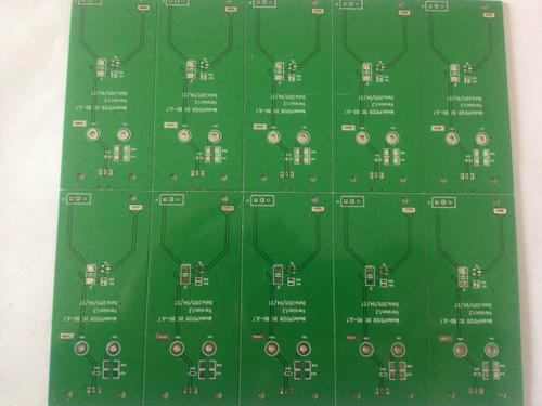
A: Component installation offset mainly refers to the position deviation in X-Y after the component is installed on the PCB. The reasons for this are as follows: (1) Reason for PCB board a: The curvature of the PCB board exceeds the allowable range of the device. The maximum upwarping is 1.2mm, and the maximum downwarping is 0.5mm. b: The height of the support pins is inconsistent, resulting in uneven support of the printed board. c: Poor flatness of workbench support platform d: Circuit board wiring has low accuracy and poor consistency, especially with significant differences between batches. (2) The suction pressure of the mounting nozzle is too low, and it should be above 400mmHG when taking out and mounting. (3) Abnormal blowing pressure during installation. (4) Abnormal or deviation in the amount of adhesive or solder paste applied. This leads to displacement during component installation or welding, resulting in deviation from the original position during high-speed
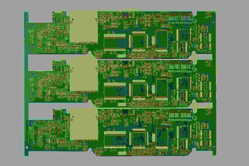
1: The optical recognition system is a fixed optical camera system. During the rotation process of the installation head, the contour of the components is recognized by the camera for optical imaging. At the same time, measure and record the center position and rotation angle of the components relative to the camera, and transmit them to the transmission control system to compare the XY coordinate position deviation and θ, Angle deviation compensation has the advantages of accuracy and flexibility, and is suitable for various specifications and shapes of components. It has a reflection recognition mode based on device electrodes, and the recognition accuracy is not affected by the size of the nozzle. Components such as SOP, QFP, BGA, PLCC generally use reflection recognition mode. The transmission recognition method is based on the shape of the component, and the recognition accuracy is affected by the size of the suction nozzle. When the shape of the suction nozzle is larger than
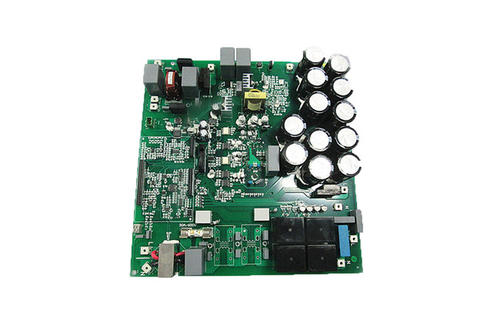
Printed circuit boards (PCBs) are an indispensable part of electronic devices, and their performance and reliability directly affect the operation of the entire system. PCB (Printed Circuit Board), also known as Printed Circuit Board (PCB) in Chinese, is an important electronic component that supports electronic components and serves as a carrier for the electrical interconnection of electronic components. Due to its use of electronic printing technology, it is called a "printed" circuit board. Cabling is a key step in PCB design, which determines the performance and stability of the circuit board. This article will explore the wiring principles and practical techniques of PCB boards to help engineers achieve better results in design. Wiring principles Following the circuit schematic diagram Wiring should strictly follow the circuit schematic to ensure correct wiring connections and prevent short or open circuit problems. During the wiring process, each component in the circuit
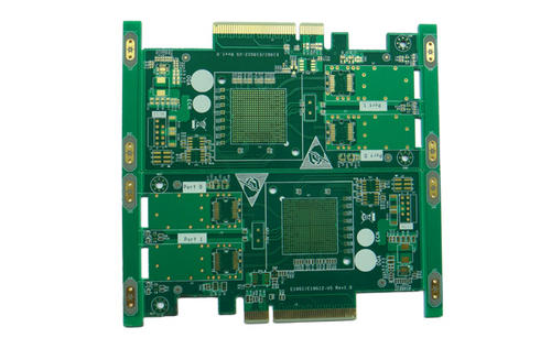
There are many knowledge points about PCB, and it is difficult for one to understand them in a short time, but basic common sense still needs to be learned quickly. So, do you understand the basic knowledge of PCB sampling? 1. PCB measurement unit The unit of measurement for PCBs is usually English units, not metric units. The units of dielectric thickness, conductor length, and width are usually in inches or mils. 1mil=0.001in, 1mil=0.0254mm The thickness of a conductor is measured in ounces (oz, where the mass of a metal conductor refers to the mass of 1 inch of material), Commonly used thickness is 0.5oz=17.5 μ m. 1.0oz=35.0 μ m. 2.0oz=70.0 μ m. 3.0oz=105.0 μ M. 2. Physical characteristics of PCB transmission lines In PCB proofing, the length L and width W of the transmission line are usually set by the PCB layout engineer. The width and spacing of transmission lines are generally not less than 5mil; The thickness H of the transmission line varies depending on the manufac
Inquiry Now

