 +86 755 2794 4155
  sales@knownpcb.com
-
Shenzhen KNOWNPCB Technology Co., Ltd.
 +86 755 2794 4155
  sales@knownpcb.com
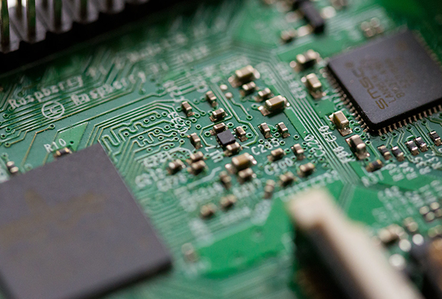
Have you noticed that now more and more of our lighting is using led lighting.What is LED? Compared to the traditional light bulbs, LEDs have lower power consumption, longer lifetime and higher energy efficiency. In the PCB industry,when we say LED PCB, it refers to the pcb used for LED lighting, if you are looking for a suitable LED PCB for your lighting system, this article may bring you something. WHAT ARE LEDS COMPOSED OF?LED is an initial light-emitting diode that produces light when an electric current passes through. LEDs typically have negative and positive electrodes, which generate light in the visible light region.The LEDS are glued to the PCB by soldering process and have electrical connections for lighting.Since light-emitting diodes dissipate a lot of heat when they are in use, when you are designing LED, the metal core is usually the best choice for LED PCB, it is because that it dissipates heat more faster. Among them, the metal material aluminum is the most widely used
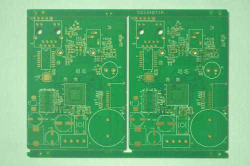
Accuracy and consistency: 5G products have increased the data signal transmission rate from 25Gbps to 56Gbps, and have put forward stricter requirements for product impedance, loss, etc. The product impedance requirement has been increased from 10% to 5%, and the line width tolerance has been increased from 20% to 10%. The impact of line flatness on the signal is also significant. From the perspective of the influencing factors of impedance control, the size of impedance tolerance is influenced by the dielectric thickness tolerance, copper thickness tolerance, and current control accuracy. As shown in the following figure, the inner layer impedance tolerance has been reduced from 10% to 5%, the dielectric thickness tolerance should be controlled at ± 7%, the copper thickness tolerance should be controlled at ± 3%, the line width tolerance should be controlled at ± 8%, and the outer layer impedance should also be controlled. This is closely related to sheet metal, PCB engineering d
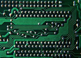
Blind hole embedding: The functionality of 5G products has been improved, and the demand for high-density PCB circuit boards has increased. There is an increasing demand for multi-stage HDI products and even products that are interconnected in any order. Currently, most PCB factories have a trend towards mature 1-3 level HDI, but higher level blind hole embedding capabilities need to be improved Stub: The short pile effect of 112G products cannot be ignored, and the back drilling stubs have put forward stricter requirements, and ostub will be the trend Copper embedding: Heat dissipation requirements for 5G communication high-frequency high-power devices. Copper blocks are embedded inside the PCB to enhance its heat dissipation capability
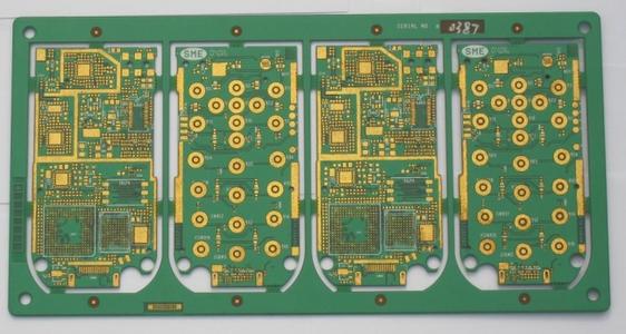
Through hole: A through hole is a hole that passes from one side of a circuit board to the other. They can completely penetrate the entire circuit board and can be soldered through pins, sockets, or other components. Through holes are usually used to connect circuits at different levels, providing electrical connections and mechanical support. Blind via: A blind hole is a hole that only enters the circuit board from one side and does not penetrate the entire board thickness. They are used to connect circuits between surface and internal layers. Blind holes can be welded to components through surface assembly technology, but cannot be connected to the other side of the circuit board through through-holes. Buried via: A buried hole is a hole completely located inside a circuit board, which neither enters or exits from one side nor penetrates the entire board thickness. Buried holes are used to connect circuits between internal layers without affecting the external surface. Buried h
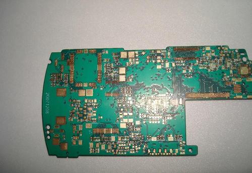
Many HDI circuit boards know that the circuit board industry is a relatively "money burning" industry, and opening a PCB factory is particularly expensive, especially for PCB companies targeting high-end products. The investment in a production line often exceeds 100 million yuan. The largest proportion of investment in PCB factories is in various types of PCB equipment. Take a look at the investment data for the following groups of projects: A major PCB project in Hubei has a total investment of 5 billion yuan, covers an area of 204 acres, and a building area of 240000 square meters, of which 1 billion yuan is invested in equipment. In August 2020, a PCB listed manufacturing enterprise issued convertible bonds to raise a net amount of 1.759 billion yuan to invest in a 1.2 million square meter multi-layer printed circuit board project in Zhuhai, with additional equipment procurement and installation costs of 1.149 billion yuan. The planned investment amount for the first phase
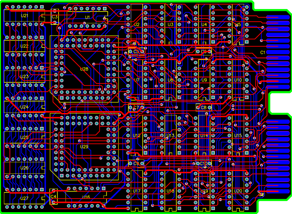
(1) Matching of expansion and contraction coefficients Generally, circuit boards are designed with a large area of copper foil for grounding purposes, and sometimes the Vcc layer also has a large area of copper foil. When these large areas of copper foil cannot be evenly distributed on the same circuit board, it will cause uneven heat absorption and dissipation speed. Of course, circuit boards will also expand and shrink, but if the expansion and contraction cannot match, it will cause different stress changes and ultimately deformation, At this point, if the temperature of the board has reached the Tg value, the board will begin to soften and become permanently deformed after curing. (2) The connection points (vias, vias) of each layer on the circuit board limit the expansion and contraction of the board Nowadays, most circuit boards are multi-layer boards, and there are connection points (through holes, blind holes, buried holes) between layers that are like rivets. In places wh
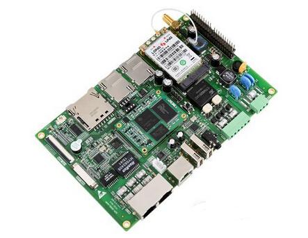
The hole in the pad refers to the hole punched on the pad, which is an SMD pad, usually referring to SMD and BGA pads of 0603 and above, commonly referred to as VIP (via in pad). The solder pad of the plug-in hole cannot be referred to as an in tray hole, as the plug-in hole solder pad requires the insertion of components for welding, and all plug-in pin solder pads have holes. With the development of electronic products in the direction of light, thin, and small, PCB boards have also been pushed towards high-density and difficult development, so the volume of components is gradually decreasing. For example, if the packaging of BGA components is small, the spacing between pins will decrease accordingly. If the pin spacing is small, it is difficult to wire the pins inside the package, and it is necessary to change layers and punch holes for wiring. When the spacing between BGA pins is small and cannot be fanout, there is only one solution, which is to drill holes in the tray. Ther
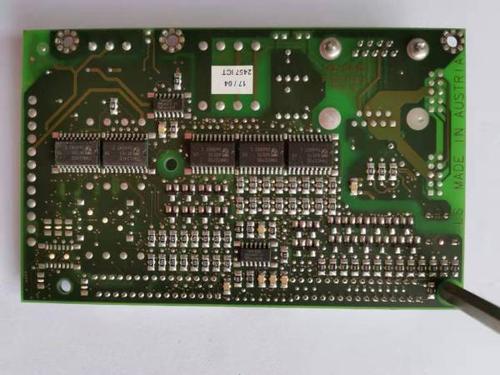
From PCB circuit board design to the completion of all component welding to a high-quality circuit board, it requires strict control from PCB design engineers, as well as the level of welding processes and workers. There are mainly the following factors: PCB board drawing, circuit board workmanship quality, device quality, oxidation degree of device pins, solder paste quality, printing quality of solder paste, accuracy of program programming of the SMT machine, mounting quality of the SMT machine, setting of temperature curve of the reflow soldering furnace, and other factors that may affect poor PCB soldering. The process of PCB drawing is an insurmountable part of the PCB chip welding factory itself. Due to the fact that circuit designers often do not solder circuit boards, they cannot gain direct welding experience and are unaware of the various factors that affect welding; The workers in the welding factory do not understand the drawing board, they only focus on completing pro
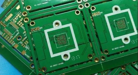
Why sometimes, even though the PCB design has not been checked for errors, there are still adverse situations such as short circuits and broken boards after production and processing? That's because you didn't consider the issue of hole spacing, which resulted in unavoidable losses during the assembly process. The production of a single or double-sided PCB panel involves drilling non through holes or through holes directly after cutting; The multi-layer board is drilled after completing the pressing plate. Drilling can be divided into: part holes, tool holes, through holes, blind holes, and buried holes according to their functions. Conventional drilling is processed through drilling machinery, and in actual processing, the spacing between drilling holes usually affects the processing of the drilling rig and the reliability of the finished product. So when designing, it is important to consider the actual machining situation of hole spacing: VIA via (commonly known as conductiv
Inquiry Now

