 +86 755 2794 4155
  sales@knownpcb.com
-
Shenzhen KNOWNPCB Technology Co., Ltd.
 +86 755 2794 4155
  sales@knownpcb.com
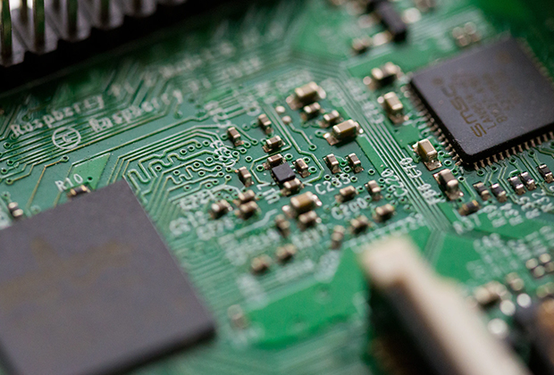
Have you noticed that now more and more of our lighting is using led lighting.What is LED? Compared to the traditional light bulbs, LEDs have lower power consumption, longer lifetime and higher energy efficiency. In the PCB industry,when we say LED PCB, it refers to the pcb used for LED lighting, if you are looking for a suitable LED PCB for your lighting system, this article may bring you something. WHAT ARE LEDS COMPOSED OF?LED is an initial light-emitting diode that produces light when an electric current passes through. LEDs typically have negative and positive electrodes, which generate light in the visible light region.The LEDS are glued to the PCB by soldering process and have electrical connections for lighting.Since light-emitting diodes dissipate a lot of heat when they are in use, when you are designing LED, the metal core is usually the best choice for LED PCB, it is because that it dissipates heat more faster. Among them, the metal material aluminum is the most widely used

1) Single panel process flow Cutting and grinding → drilling → outer layer graphics → (full plate gold plating) → etching → inspection → silk screen welding resistance → (hot air leveling) → silk screen characters → contour processing → testing → inspection 2) Process flow of double-sided tin spraying board Cutting and grinding → drilling → copper sinking and thickening → outer layer graphics → tin plating, etching and tin removal → secondary drilling → inspection → silk screen resistance welding → gold-plated plug → hot air leveling → silk screen characters → external processing → testing → inspection 3) Process flow of nickel gold plating on double-sided boards Cutting and grinding → drilling → copper sinking and thickening → outer layer graphics → nickel plating, gold film removal and etching → secondary drilling → inspection → silk screen resistance welding → silk screen characters → external processing → testing → inspection 4) Process flow of multi-layer tin spraying bo
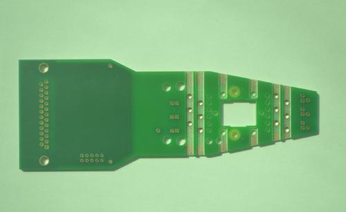
The names of circuit boards include: ceramic circuit boards, alumina ceramic circuit boards, aluminum nitride ceramic circuit boards, circuit boards, PCB boards, aluminum substrates, high-frequency boards, thick copper plates, impedance boards, PCBs, ultra-thin circuit boards, ultra-thin circuit boards, printed (copper etching technology) circuit boards, etc. Circuit boards make circuits miniaturized and intuitive, playing an important role in the mass production of fixed circuits and optimizing the layout of electrical appliances. A circuit board can be called a printed circuit board or a printed circuit board, with the English name "Printed Circuit Board" PCB (Flexible Printed Circuit Board) FPC circuit board (FPC circuit board, also known as flexible circuit board) is a highly reliable and excellent flexible printed circuit board made of polyimide or polyester film as the substrate. It has the characteristics of high wiring density, light weight, thin thickness, and good bending p

The circuit processing of multi-layer PCBs is no different from that of single-layer and double-layer PCBs, but the biggest difference lies in the through hole process. The circuits are all etched, and the via holes are drilled and then plated with copper. Everyone involved in hardware development understands these, so we won't go into detail. Multilayer circuit boards typically include through hole boards, first order boards, second order boards, and second order stacked hole boards. Higher level boards such as third-order boards and arbitrary layer interconnection boards are rarely used in daily life, and their prices are quite expensive. We won't discuss them much for now. In general, 8-bit microcontroller products use 2-layer through-hole boards; Intelligent hardware at the 32-bit microcontroller level, using 4-6-layer through-hole boards; Intelligent hardware at the Linux and Android levels, using 6-layer through holes to 8-layer first-order HDI boards; Compact products lik
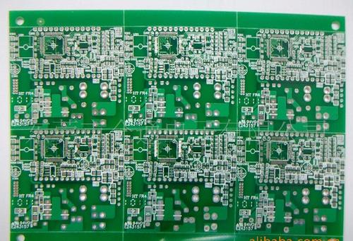
1. The meaning of the solder mask layer is to open a window on the green oil of the entire solder mask, in order to allow welding! 2. By default, areas without solder mask must be coated with green oil! 3. Paste mask layer for SMD packaging! SMT encapsulation uses: toplayer layer, topsolver layer, toppaste layer, and the toplayer is the same size as the toppaste layer, but the topsolver is one circle larger than them. DIP encapsulation only uses the top layer and multi layer layers (after some decomposition, I found that the multi layer layer is actually the top layer, bottomlayer, top layer, and bottomlayer layers with overlapping sizes), and the top layer/bottomlayer is one circle larger than the top layer/bottomlayer. Question: Is the statement 'tin or gold plating only occurs when the copper layer corresponding to the solder layer has copper' correct? This sentence is from a person who works in a PCB factory. His meaning is: to make the effect of tin plating on the part pain
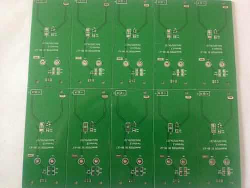
Protel 99 SE provides 16 mechanical layers, which are generally used to set the overall dimensions, data markers, alignment markers, assembly instructions, and other mechanical information of circuit boards. These information may vary depending on the requirements of the design company or PCB manufacturer. Executing the menu command Design | MechanicalLayer can set more mechanical layers for the circuit board. In addition, the mechanical layer can be attached to other layers to output the display together. 4 Solder mask layer Apply a layer of paint, such as solder mask, to various areas outside the solder pad to prevent tin from being applied to these areas. The solder mask layer is used to match the solder pad during the design process and is automatically generated. Protel 99 SE provides two solder mask layers: Top Solder and Bottom Solder. 5 Paste mask layer Its function is similar to that of the solder mask layer, except for the corresponding bonding pads of surface mounted
The volume of electronic products is becoming increasingly thin and short, and directly stacking holes on through blind holes is a design method to achieve high-density interconnection. To do a good job of stacking holes, the first step is to ensure the flatness of the hole bottom. There are several production methods, and the electroplating hole filling process is one of the representative ones. Next, let the PCB engineer teach you about the PCB electroplating hole filling process. 1. Advantages of electroplated hole filling: (1) Beneficial for designing stacked holes and holes on the disc; (2) Improving electrical performance helps with high-frequency design; (3) Helps to dissipate heat; (4) Plug holes and electrical interconnections are completed in one step; (5) The blind hole is filled with electroplated copper, which has higher reliability and better conductivity than conductive adhesive. 2. Physical impact parameters The physical parameters that need to be studied in

On PCBs, nickel is used as a substrate coating for precious and base metals. The deposition layer of low stress nickel on PCB is usually prepared using modified Watt nickel plating solution and some amino sulfonic acid nickel plating solution with stress reducing additives. What are the common problems encountered when using PCB nickel plating solution, as analyzed by CITIC Huawei? 1、 Temperature - Different nickel processes use different plating bath temperatures. In nickel plating solutions with higher temperatures, the obtained nickel coating has low internal stress and good ductility. The general operating temperature is maintained at 55-60 degrees Celsius. If the temperature is too high, nickel salt hydrolysis will occur, causing pinholes in the coating and reducing cathodic polarization. 2、 PH value - The pH value of nickel plating electrolyte has a significant impact on the performance of the coating and electrolyte. The pH value of PCB nickel plating electrolyte is genera
The volume of electronic products is becoming increasingly thin and short, and directly stacking holes on through blind holes is a design method to achieve high-density interconnection. To achieve good hole stacking, the first step is to ensure the flatness of the hole bottom. There are several typical methods for making flat hole surfaces, and electroplating hole filling process is one of the representative ones. The electroplating hole filling process can not only reduce the necessity of additional process development, but also be compatible with current process equipment, which is conducive to achieving good reliability. So, what factors affect the PCB electroplating hole filling process? In PCB sampling, the influence of substrate on electroplating hole filling cannot be ignored, generally including factors such as dielectric layer material, hole shape, thickness to diameter ratio, and chemical copper coating. (1) Medium layer material. The material of the dielectric layer ha
Inquiry Now

