 +86 755 2794 4155
  sales@knownpcb.com
-
Shenzhen KNOWNPCB Technology Co., Ltd.
 +86 755 2794 4155
  sales@knownpcb.com
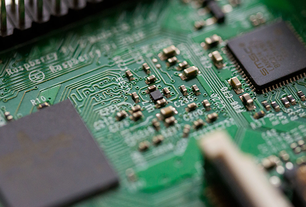
Have you noticed that now more and more of our lighting is using led lighting.What is LED? Compared to the traditional light bulbs, LEDs have lower power consumption, longer lifetime and higher energy efficiency. In the PCB industry,when we say LED PCB, it refers to the pcb used for LED lighting, if you are looking for a suitable LED PCB for your lighting system, this article may bring you something. WHAT ARE LEDS COMPOSED OF?LED is an initial light-emitting diode that produces light when an electric current passes through. LEDs typically have negative and positive electrodes, which generate light in the visible light region.The LEDS are glued to the PCB by soldering process and have electrical connections for lighting.Since light-emitting diodes dissipate a lot of heat when they are in use, when you are designing LED, the metal core is usually the best choice for LED PCB, it is because that it dissipates heat more faster. Among them, the metal material aluminum is the most widely used
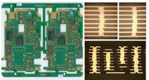
1. One on one assembly board One on one splicing is the simplest splicing method, suitable for small PCB boards with a small quantity. Arrange each small board accurately on the large board according to the design requirements, then perform one-time etching, cutting, and other processes, and finally cut the large board into multiple independent small boards. This method is suitable for sample production or small-scale production, but it is inefficient for large-scale production. 2. Minimize Area Splicing Minimizing area splicing is an optimized splicing method. Arrange multiple small boards on the large board in a certain way to minimize the area of the large board and save materials. This method is suitable for large-scale production, which can improve utilization and reduce costs. 3. Maximize the number of pieces for splicing Maximizing the number of pieces is a splicing method that pursues production efficiency. According to the size and process requirements of the small bo
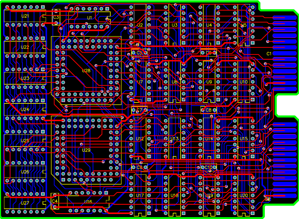
What are the advantages of the product? One is automation. It can be connected to the production line of circuit boards, achieving functions such as automatic feeding, automatic detection, and automatic identification of good and bad products, without the need for manual operation, greatly reducing labor costs and reducing quality damage caused by manual operation. Secondly, high accuracy. Adopting high-precision CIS scanning system, as well as technologies such as automatic positioning, image processing, and intelligent detection and analysis, to achieve high-precision detection. Thirdly, high efficiency. Equipped with a multi-channel detection device, it can customize 3 and 6 channels for simultaneous detection, greatly improving detection efficiency.
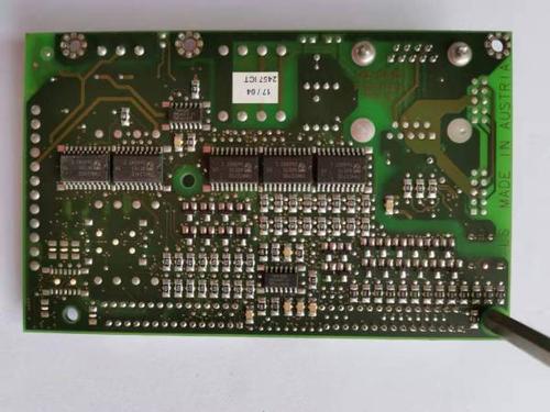
The main problem with RF circuit layout is usually the unsatisfactory characteristic impedance of the circuit, including circuit components and their interconnections. If the copper layer on the lead is relatively thin, it is equivalent to an inductance line and forms a distributed capacitance with other adjacent leads. When the lead passes through a through hole, it also exhibits inductance and capacitance characteristics. The through-hole capacitance mainly comes from the capacitance formed between the copper coating on the through-hole pad side and the copper coating on the formation, which is separated by a relatively small circular ring. Another influence comes from the cylindrical structure of the metal through hole itself. The influence of parasitic capacitance is generally small and usually only causes the edge of high-speed digital signals to deteriorate. The biggest impact of via is the parasitic inductance caused by the corresponding interconnection method. Because in
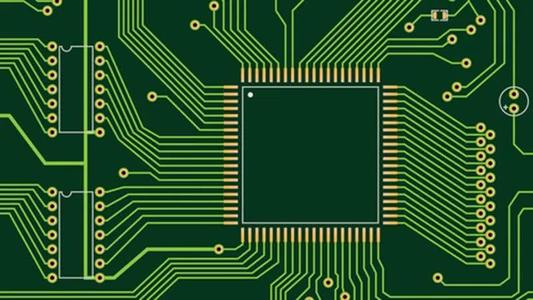
1. High precision: CCD automatic alignment, automatic expansion and contraction to ensure printing accuracy. The maximum printing resolution is 1440dpi. 2. Fine text: Using well-known brand inkjet printing heads for more precise printing quality. Minimum text size 500 μ M/400 μ m. Minimum line width 75 μ M/60 μ M. 3. High efficiency: The multi line inkjet printing head has a higher printing speed. 4. Short cycle: No need to make screen printing, three steps in place, shortening the production cycle. 5. The spray printing area has strong inclusivity: the maximum spray printing area is 610 * 762mm, and the thickness range of the circuit board is 0.1-10mm, with strong inclusivity. 6. Multi spray printing mode: mass production, high-precision, and custom mode. 7. Cost saving: Eliminating various equipment and material costs, as well as labor costs, in the wire mesh process. 8. More environmentally friendly: It does not produce pollutants and is friendly to the environment and op
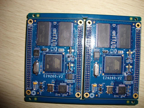
In recent years, people have increasingly attached importance to environmental protection, so while demanding steady economic development, there are also more requirements for environmental protection construction. Building an "environmentally friendly" society has increasingly become an urgent need for people. The country has also increased its efforts to regulate environmental protection to meet the needs of the times. In 2017, China comprehensively strengthened environmental emission restrictions and conducted inspections on the manufacturing industry, forcing nearly a hundred enterprises to suspend trading for rectification. In 2018, the implementation of the "Environmental Protection Tax" resulted in an increase in environmental protection costs for PCB manufacturers. After a round of rectification, some PCB manufacturers who could not meet environmental requirements were forced to withdraw from the market, and those fortunate enough to survive also had higher requirements fo
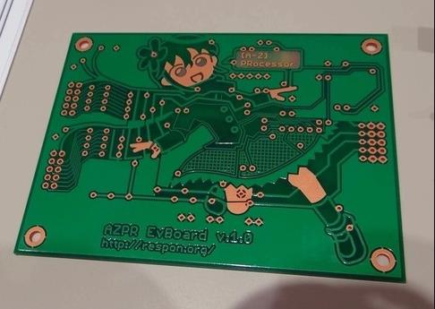
If two holes are too close during drilling operation, it will affect the efficiency of PCB drilling process. Due to the fact that after drilling the first hole, the material in one direction is too thin when drilling the second hole, resulting in uneven stress on the drilling nozzle and uneven heat dissipation of the drilling nozzle, leading to the breakage of the drilling nozzle, resulting in unsightly PCB hole collapse or incomplete drilling. 2. In PC multilayer boards, vias have hole rings on each layer of the circuit, and the environment around each layer of the hole ring varies, with and without wire clips. When optimizing files in PCB factory CAM engineers, they will cut off a portion of the hole ring in cases where the clamping wire is too close or the hole is too close to the hole, to ensure a safe distance of 3mil between the welding ring and different network copper/wire. 3. The hole position tolerance for drilling is ≤ 0.05mm. When the tolerance reaches the upper limit
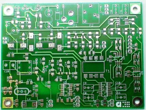
The first level is relatively simple, and the process and process are easy to control. The second order problem starts to get troublesome, one is the alignment problem, and the other is the punching and copper plating problem. There are various second-order designs, one of which is to stagger the positions of each stage and connect the secondary layers through wires in the middle layer, which is equivalent to two first-order HDIs. The second method is to overlap two first order holes and achieve second order through superposition. The processing is also similar to two first order holes, but there are many process points that need to be specially controlled, which is mentioned above. The third method is to directly drill holes from the outer layer to the third layer (or N-2 layer), with many different processes and greater difficulty in drilling. For the third order, the second order analogy is.
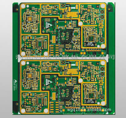
PCB (Printed Circuit Board), also known as Printed Circuit Board in Chinese, is an important electronic component that supports electronic components and serves as the carrier for electrical connections of electronic components. Due to its use of electronic printing technology, it is called a "printed" circuit board. Its main function is to avoid manual wiring errors due to the consistency of similar printed boards in electronic equipment, and to achieve automatic insertion or installation of electronic components, automatic soldering, and automatic detection, ensuring the quality of electronic equipment, improving labor productivity, reducing costs, and facilitating maintenance. HDI boards refer to high-density interconnect circuit boards. The boards with blind hole electroplating and secondary pressing are all HDI boards, which are divided into first, second, third, fourth, and fifth order HDIs. For example, the motherboard of the iPhone 6 is a fifth order HDI. Simply burying
Inquiry Now

