 +86 755 2794 4155
  sales@knownpcb.com
-
Shenzhen KNOWNPCB Technology Co., Ltd.
 +86 755 2794 4155
  sales@knownpcb.com
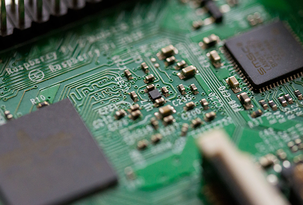
Have you noticed that now more and more of our lighting is using led lighting.What is LED? Compared to the traditional light bulbs, LEDs have lower power consumption, longer lifetime and higher energy efficiency. In the PCB industry,when we say LED PCB, it refers to the pcb used for LED lighting, if you are looking for a suitable LED PCB for your lighting system, this article may bring you something. WHAT ARE LEDS COMPOSED OF?LED is an initial light-emitting diode that produces light when an electric current passes through. LEDs typically have negative and positive electrodes, which generate light in the visible light region.The LEDS are glued to the PCB by soldering process and have electrical connections for lighting.Since light-emitting diodes dissipate a lot of heat when they are in use, when you are designing LED, the metal core is usually the best choice for LED PCB, it is because that it dissipates heat more faster. Among them, the metal material aluminum is the most widely used
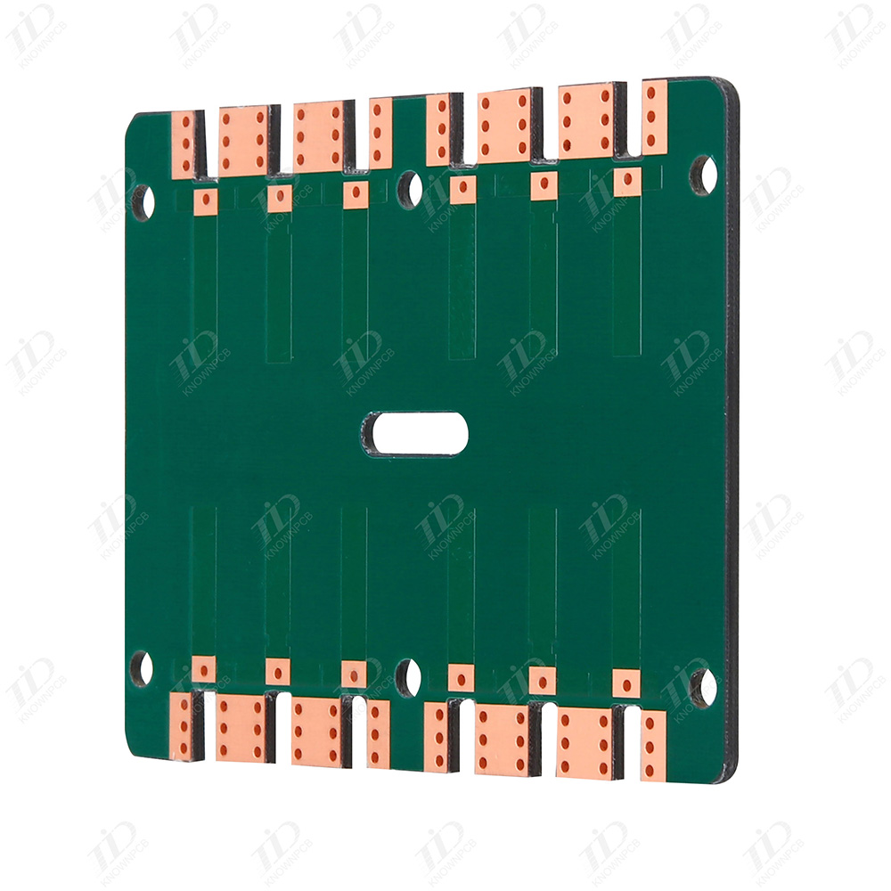
1. Material selection specifications: Medical PCB boards must be made of materials that comply with medical industry standards. These materials need to undergo strict safety and reliability testing to avoid any negative impact on patient health. 2. Electrical performance specifications: Medical PCB boards need to have good electrical performance, including stable voltage output, low noise, and low power consumption. These performance requirements are achieved through appropriate design and high-quality components to ensure the normal operation and accuracy of medical equipment. 3. Environmental adaptability specifications: Medical equipment may be affected by various environmental conditions during use, including temperature, humidity, and vibration. Therefore, medical PCB boards need to have good environmental adaptability to ensure reliability and stability under various extreme conditions. 4. Production process specifications: The production of medical PCB boards needs to
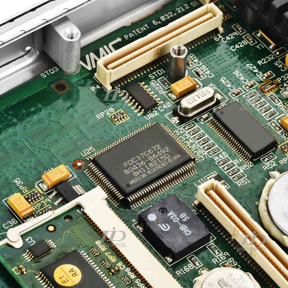
1. Appearance inspection: Check whether the tin material is intact, whether there are obvious crystalline, powdery, fibrous and other foreign objects, and whether there are drag marks, spots and other phenomena. 2. Wet tensile test: Check the tensile strength, elongation at break, and modulus at break of the tin material. 3. Wet bending test: Check the bending strength and fracture modulus of the tin material. 4. Hot tempering test: Check the heat resistance of the tin material. 5. Resistivity test: Check the resistivity of the tin material. 6. Corrosion resistance inspection: Detect the corrosion resistance of the tin material, check whether there is agglomeration and corrosion phenomenon in the tin material. 7. Surface corrosion resistance test: Check the surface corrosion resistance of the tin material and check for any corrosion marks on the surface.
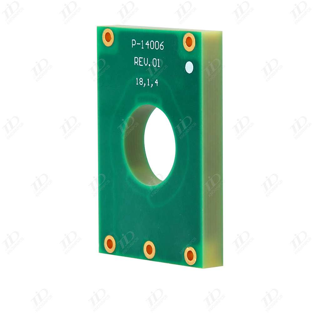
The influence of welding process parameters on the surface quality of welding is quite complex, mainly including the following key points: 1. Control of preheating temperature The function of preheating: ① Fully volatilize the solvent in the soldering flux to avoid affecting the wetting of the printed board and the formation of solder joints when the printed board passes through soldering; ② Bring the printed circuit board to a certain temperature before welding to prevent warping and deformation caused by thermal shock. Based on our experience, the preheating temperature is generally controlled at 180 200 ℃ and the preheating time is 1-3 minutes. 2. Welding rail inclination angle The inclination angle of the track has a significant impact on the welding effect, especially when welding high-density SMT devices. When the inclination angle is too small, bridging is more likely to occur, especially in welding, where the "shielding area" of SMT devices is more prone to bridging; If
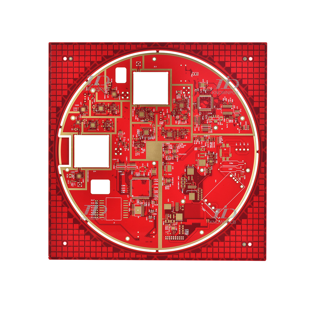
In wave soldering, the main process materials used are flux and solder. 1. The application of flux can remove oxides from the welding surface, prevent reoxidation of the solder and welding surface during welding, reduce the surface tension of the solder, and help transfer heat to the welding area. Flux plays a crucial role in controlling welding quality. At present, the most commonly used flux for wave soldering is non cleaning flux, and there are the following requirements when selecting flux: (1) The melting point is lower than that of solder; (2) The infiltration diffusion speed is faster than that of melted solder; (3) The viscosity and specific gravity are smaller than those of solder; (4) Stable storage at room temperature. 2. Quality control of solder Tin lead solder continuously oxidizes at high temperatures (250 ℃), causing a continuous decrease in the tin content of the tin lead solder in the tin pot, deviating from the eutectic point, resulting in poor flowability
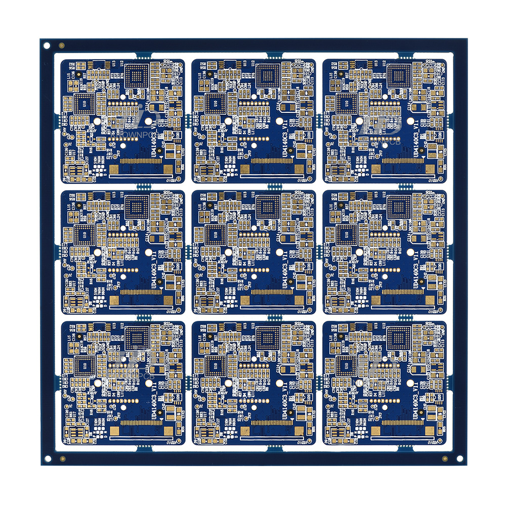
1. Pad design (1) When designing plug-in component pads, the pad size should be designed appropriately. If the solder pad is too large, the solder spreading area is large, and the formed solder joints are not full, while the surface tension of the smaller solder pad copper foil is too small, and the formed solder joints are non wetting solder joints. The fit gap between the aperture and the component lead is too large, which is prone to false soldering. When the aperture is 0.05-0.2mm wider than the lead and the diameter of the solder pad is 2-2.5 times the aperture, it is an ideal welding condition. (2) When designing solder pads for SMD components, the following points should be considered: in order to eliminate the "shadow effect" as much as possible, the solder end or pin of SMD should be facing the direction of the tin flow to facilitate contact with the tin flow and reduce false soldering and solder leakage. For smaller components, they should not be placed behind larger co
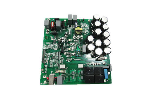
In recent years, with the continuous development of electronic products and the further advancement of intelligence, the design of printed circuit boards (PCBs) has become increasingly important. The design of PCB multilayer structure occupies a core position in modern electronic equipment, and its rationality directly affects the performance and reliability of electronic products. Firstly, let's take a look at the design principles of a multi layer PCB structure. Firstly, the selection of layers is very important. The more layers there are, the higher the complexity of signal transmission, so a balance between circuit complexity, electromagnetic interference, and cost needs to be considered in the design. Secondly, in the design of PCB multilayer boards, the signal circuits of each layer should be reasonably arranged. There should be sufficient spacing between different signal lines to avoid mutual interference. In order to improve the speed of signal transmission and reduce ele
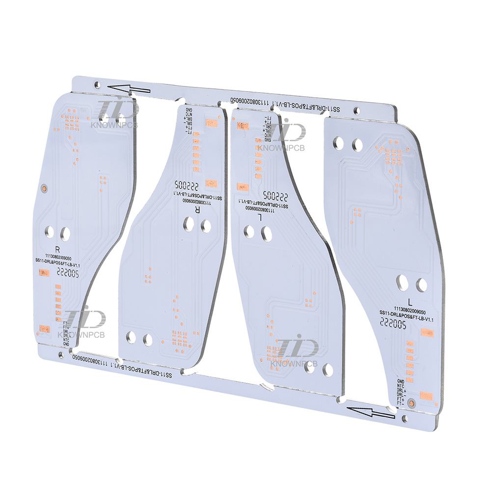
With the continuous development of technology, LED circuit boards are playing an increasingly important role in the lighting industry. They not only provide high brightness lighting effects, but also have advantages such as energy conservation, environmental protection, and long service life. In order to further promote the development of LED light circuit boards, new design trends are constantly emerging. Today, the editor will delve into the current 5 cutting-edge LED light board PCB design trends and look forward to the possibilities that technology can bring to the future. Firstly, customized design has become mainstream. Traditionally, the design of LED light circuit boards has been relatively uniform, but now the market demand is constantly personalized, and people's requirements for lighting are becoming increasingly diverse. Therefore, more and more lamp panel manufacturers are providing customized design services to meet the needs of different customers. Customized desig
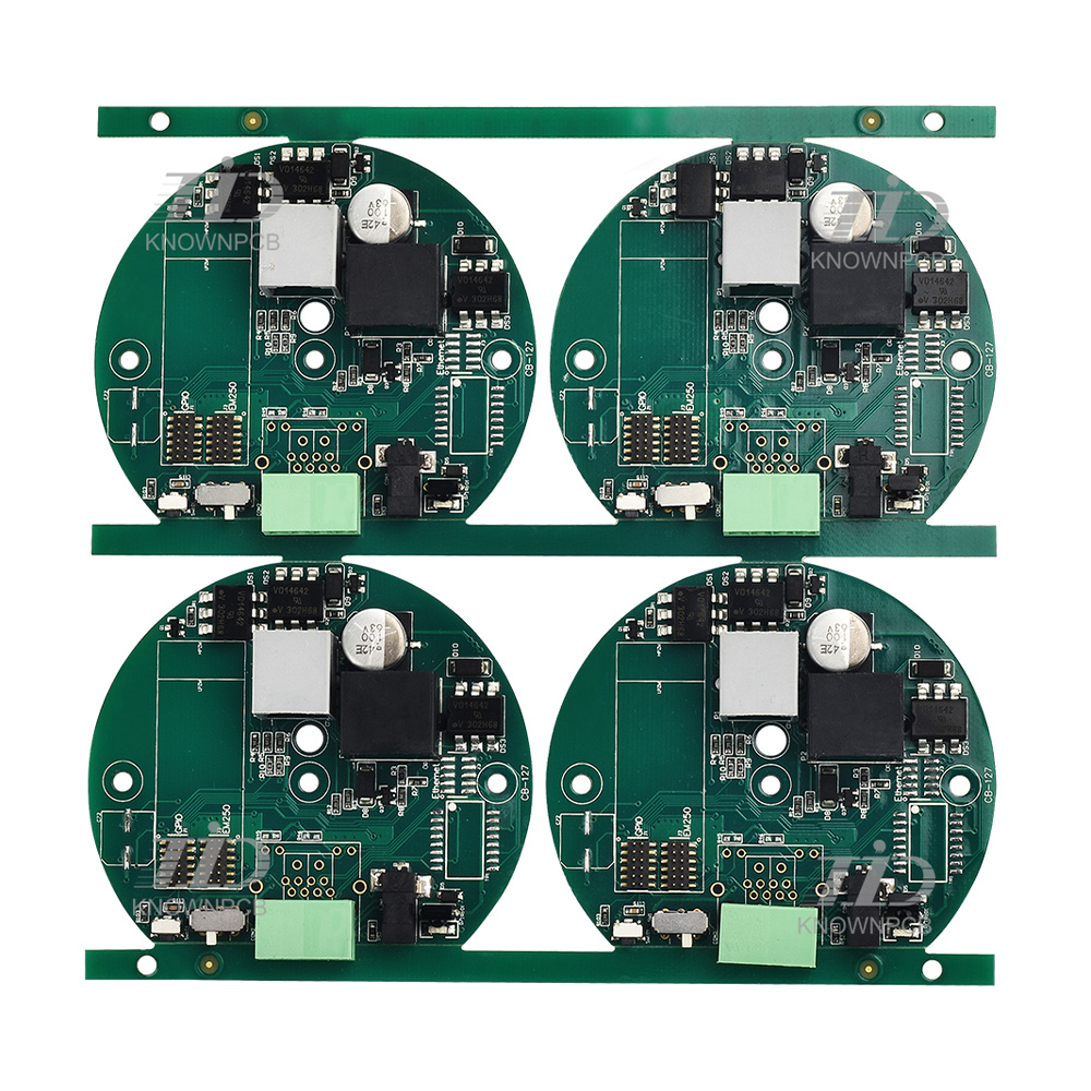
Firstly, the first step in the production of new energy vehicle PCB boards is the design of circuit board drawings. The designer draws the layout and circuit connection drawings of the circuit board based on the functional and dimensional requirements of the electronic equipment of the new energy vehicle. The accuracy and rationality of design drawings are crucial for the subsequent manufacturing process. Next is the plate making and electroplating of the circuit board. Plate making is the process of transferring design drawings to photoresist through lithography technology, and then gradually exposing the copper layer through chemical corrosion to form the required circuit lines. Next, the copper plate is immersed in an electroplating bath, and through the action of current, a layer of copper foil is formed on the circuit line to enhance conductivity and durability. The third key step is drilling and deburring. In this step, the high-speed drilling on the small lathe drills n
Inquiry Now

