 +86 755 2794 4155
  sales@knownpcb.com
-
Shenzhen KNOWNPCB Technology Co., Ltd.
 +86 755 2794 4155
  sales@knownpcb.com
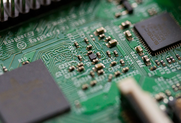
Have you noticed that now more and more of our lighting is using led lighting.What is LED? Compared to the traditional light bulbs, LEDs have lower power consumption, longer lifetime and higher energy efficiency. In the PCB industry,when we say LED PCB, it refers to the pcb used for LED lighting, if you are looking for a suitable LED PCB for your lighting system, this article may bring you something. WHAT ARE LEDS COMPOSED OF?LED is an initial light-emitting diode that produces light when an electric current passes through. LEDs typically have negative and positive electrodes, which generate light in the visible light region.The LEDS are glued to the PCB by soldering process and have electrical connections for lighting.Since light-emitting diodes dissipate a lot of heat when they are in use, when you are designing LED, the metal core is usually the best choice for LED PCB, it is because that it dissipates heat more faster. Among them, the metal material aluminum is the most widely used
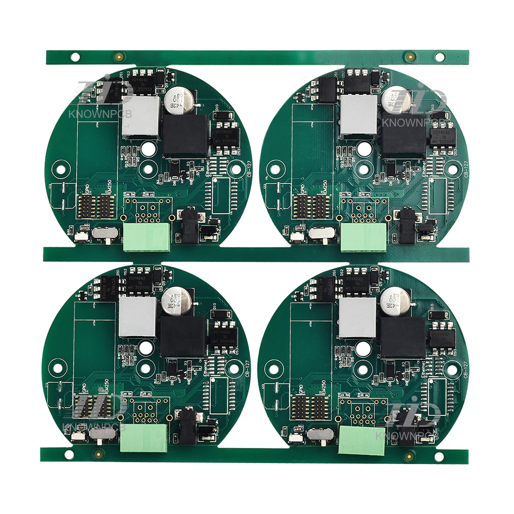
Firstly, a challenge in the design of switch PCB circuit boards is the issue of signal interference. On PCB boards, the generation and transmission of high-speed signals can generate a significant amount of electromagnetic radiation and mutual inductance. And these radiation and mutual inductance can interfere with other signals, leading to a decrease in communication signal quality. To solve this problem, we can adopt the following strategies: first, reasonably plan the routing of signal and power lines, and minimize the possibility of crossing each other; Secondly, reasonable layout and use of shielding covers and other measures to reduce the propagation of signal interference; Finally, design the grounding wire and shielding ground reasonably to improve the continuity and shielding effect of the grounding wire. Another difficulty in the design of switch PCB circuit boards is the transmission of high-speed signals. Due to the high frequency of high-speed signals in switches, p
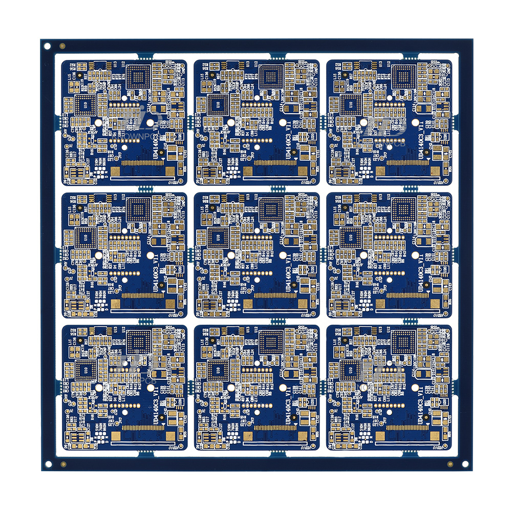
In the design and manufacturing process of PCB circuit boards, step holes are a common and important component. It plays a crucial role in the connection between electronic devices and circuit boards, so understanding the design and manufacturing principles of step holes is one of the essential skills for every electronic engineer and PCB designer. Firstly, let's introduce the basic concepts and functions of step holes. Step holes are holes with different diameters that serve as connections between electronic devices and soldering pins on PCB boards. It is usually composed of two or more cylindrical holes, forming a progressive structure layer by layer, which can effectively bear the stress during welding and connection processes and improve the reliability of the connection. When making step holes, it is first necessary to carry out appropriate design. The design includes selecting appropriate aperture and spacing, as well as determining parameters such as plate thickness and
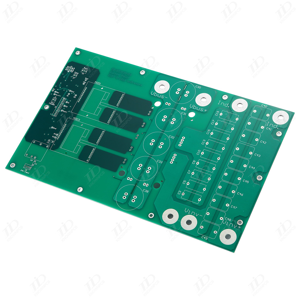
Firstly, the production of PCB boards usually starts with design. The designer conducts detailed design work based on the functional requirements of the smartphone, combined with electronic schematic and layout diagrams. Designers need to consider various factors such as signal transmission, power supply, and circuit isolation to ensure the stable and reliable performance of the PCB board. After the design is completed, the next step is the sampling stage of the PCB board. The production of PCB boards requires the use of electrical discharge machining technology, photolithography technology, chemical etching technology, and electroplating technology. Firstly, based on the designed CAD drawings, the pattern is transferred to a fiberglass board covered with copper foil using photolithography technology. Next, through chemical etching technology, unnecessary copper foil is etched away, leaving the required circuit; Then, using electroplating technology to increase the conductivity
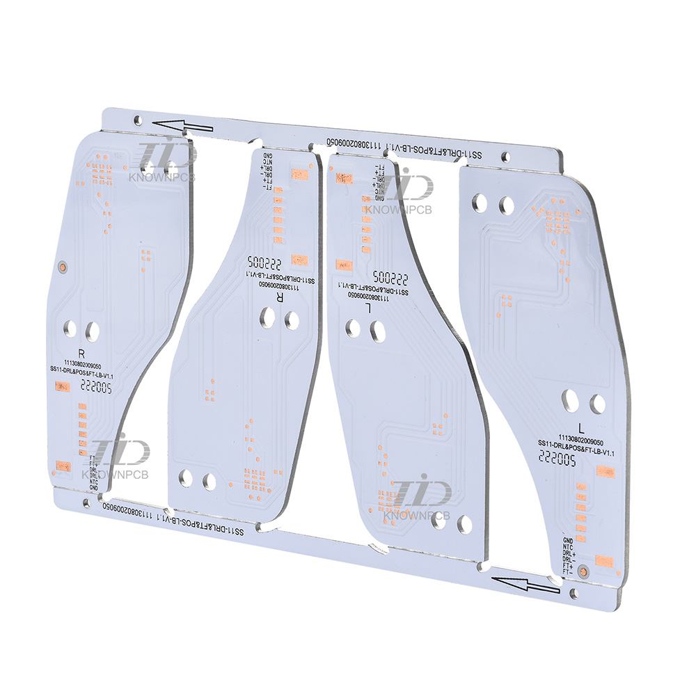
1、 V-shaped cutting and splitting process The V-shaped cutting and splitting process uses a V-shaped cutting tool to cut V-shaped grooves on both sides of the circuit board, and then break the circuit board to separate it. This process is suitable for most general board splitting needs, with simple operation and low cost. However, its disadvantage is that it is prone to cutting burrs and uneven board edges, making it suitable for circuit boards with no connectors or components on the edges. 2、 Machine milling and cutting process The machine milling and cutting process involves using a CNC machine tool for cutting and performing milling operations according to a predetermined cutting path. It can more accurately control the position and size of the split board, suitable for complex split board requirements. The edges after milling are smooth and flat, and can be directly used for welding. However, the machine milling and cutting process has a high cost and is not suitable for hig

When choosing the thickness of a PCB board, there are several main considerations to consider. 1. Mechanical strength A thinner PCB board usually has lower mechanical strength, while a thicker board will be more sturdy. Therefore, in application scenarios with high mechanical strength requirements, choosing a thicker PCB board thickness is more appropriate. 2. Welding performance The thickness of the PCB board also affects the welding performance. A thinner plate thickness can provide better thermal conductivity, making it easier to dissipate heat during the welding process. A thicker plate thickness can provide better welding strength. Therefore, in application scenarios involving welding, it is necessary to choose the appropriate PCB board thickness based on specific welding needs. 3. Cost and Space Restrictions Thicker plate thicknesses generally increase costs and occupy more space. In some application scenarios with cost and space limitations, it is necessary to choose a

In addition to the above considerations, the thickness of the PCB board also involves some details in the PCB manufacturing process. 1. Selection of PCB materials Choosing different PCB materials can affect the standard and range of PCB board thickness. For example, the thickness range of PCB boards made of FR-4 material is generally between 0.4mm and 6.0mm. 2. Thickness of Laminate (Multi Layer PCB) For multi-layer PCBs, the board thickness is generally the sum of the thicknesses of each laminate. For example, for a 4-layer PCB, if the thickness of each laminate is 0.2mm, then the thickness of the entire PCB is 0.8mm. 3. Special needs In some special application scenarios, very thin or very thick PCB board thickness may be required. For example, some flexible PCBs (FlexPCBs) can have a board thickness of less than 0.1mm, while some high-power electronic devices may require a thicker board thickness to ensure heat dissipation.

The medical industry has high requirements for the reliability and safety of electronic devices. As an important component of medical equipment, medical PCB boards have correspondingly high standards and requirements to ensure the normal operation of medical equipment and the safety of patients. Let's take a look at some specifications and standards for medical PCB boards. 1. Material selection specifications: Medical PCB boards must be made of materials that comply with medical industry standards. These materials need to undergo strict safety and reliability testing to avoid any negative impact on patient health. 2. Electrical performance specifications: Medical PCB boards need to have good electrical performance, including stable voltage output, low noise, and low power consumption. These performance requirements are achieved through appropriate design and high-quality components to ensure the normal operation and accuracy of medical equipment. 3. Environmental adaptability
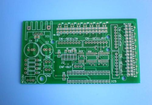
PCB circuit board reflow soldering is one of the common welding methods in the electronic assembly process. It firmly fixes electronic components on the PCB board by applying appropriate heat and melted solder paste to pre arranged welding points. However, some common problems may also arise during the reflow soldering manufacturing process. Introduce these issues and corresponding solutions. 1、 Tin splashing on the board surface Problem description: Tin splashing on the board refers to the excessive amount of solder around the welding point during reflow soldering. This may cause damage to components near the welding point, and even cause short circuits or welding failures. Solution: There are several methods to solve the problem of tin splashing on the board surface. Firstly, check whether the size and position of the welding points are appropriate to avoid excessive soldering caused by design defects. Secondly, adjust the temperature and speed in the reflow soldering furnace
Inquiry Now

