 +86 755 2794 4155
  sales@knownpcb.com
-
Shenzhen KNOWNPCB Technology Co., Ltd.
 +86 755 2794 4155
  sales@knownpcb.com
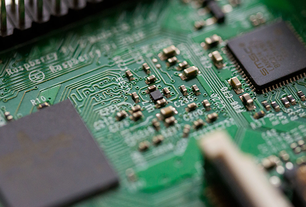
Have you noticed that now more and more of our lighting is using led lighting.What is LED? Compared to the traditional light bulbs, LEDs have lower power consumption, longer lifetime and higher energy efficiency. In the PCB industry,when we say LED PCB, it refers to the pcb used for LED lighting, if you are looking for a suitable LED PCB for your lighting system, this article may bring you something. WHAT ARE LEDS COMPOSED OF?LED is an initial light-emitting diode that produces light when an electric current passes through. LEDs typically have negative and positive electrodes, which generate light in the visible light region.The LEDS are glued to the PCB by soldering process and have electrical connections for lighting.Since light-emitting diodes dissipate a lot of heat when they are in use, when you are designing LED, the metal core is usually the best choice for LED PCB, it is because that it dissipates heat more faster. Among them, the metal material aluminum is the most widely used
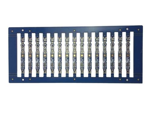
To solve the above problems of gilded boards, PCBs using gilded boards mainly have the following characteristics: 1. Due to the different crystal structures formed by depositing gold and gilding, the deposited gold will appear golden yellow and more yellow than gilding, resulting in better customer satisfaction. 2. Due to the different crystal structures formed by sinking gold and gold plating, sinking gold is easier to weld than gold plating, which will not cause poor welding and cause customer complaints. 3. Due to the fact that only nickel gold is present on the solder pad of the sinking gold plate, the signal transmission in the skin effect is not affected by the copper layer. 4. Due to the denser crystal structure of precipitated gold compared to gold plating, it is less prone to oxidation. 5. Due to the fact that only nickel gold is present on the solder pad of the sinking gold plate, it will not produce gold wire causing slight shortness. 6. Due to the fact that only n
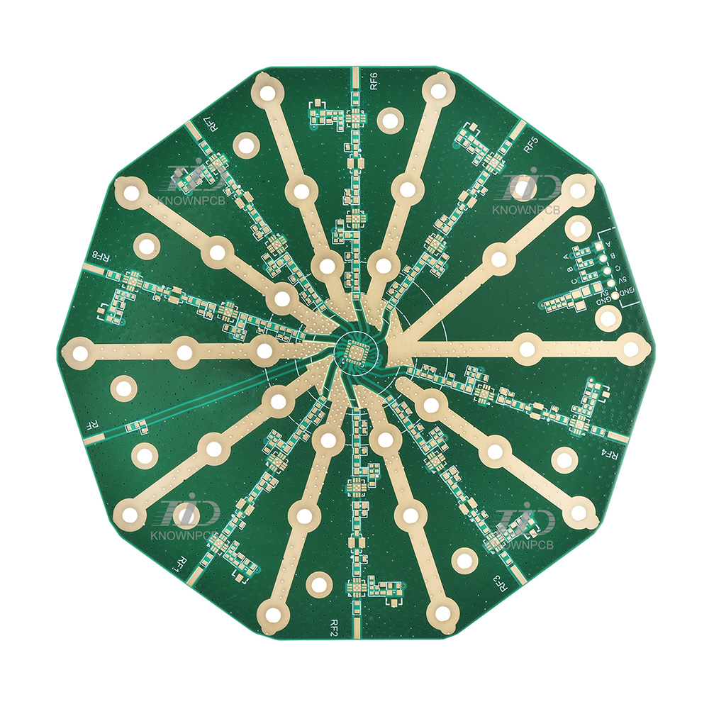
As the integration level of ICs increases, PCB sampling manufacturers also have more and more IC pins. The vertical tin spraying process makes it difficult to blow the fine solder pads flat, which brings difficulty to SMT installation; In addition, the shelf life of the tin spray board is very short. And the gilded plate precisely solves these problems: 1. For surface mount processes, especially for 0603 and 0402 ultra small surface mount processes, the flatness of the solder pad directly affects the quality of the solder paste printing process and plays a decisive role in the subsequent reflow welding quality. Therefore, whole plate gilding is often seen in high-density and ultra small surface mount processes. In the trial production stage, the influence of factors such as component procurement is often not that the board is welded immediately upon arrival, but rather that it often needs to wait for several weeks or even months before use. The shelf life of gold-plated boards is l
Single and double-sided PCB circuit boards are the most common and simple PCB boards in the printed circuit board industry. Due to their single panel design and wide circuit design, they are very easy to make. Some simple single panels can be visually inspected without testing costs. During the circuit board quotation process, it was found that there are still a few friends who are not very familiar with the differences between the two, For this reason, I would like to give you a brief introduction on the basic differences between single and double sided circuit boards! What is a PCB single panel: A PCB single panel refers to a circuit board with only one side printed with a circuit, while the other side shows no circuit (note: the other side shows PCB substrate without copper coating); What is a PCB double-sided board: A PCB double-sided board refers to a board that has printed circuits on both sides, and a small number of boards have only one side printed with circuits, while t
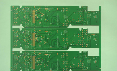
By looking at the cut surface of a PCB board to obtain a four layer board, this method is actually quite difficult, and few people have this kind of vision. However, by observing the guide holes, a four layer board can be identified. If the same guide holes can be found on both sides of the PCB board, or if the motherboard or display card is facing the light source, and the position of the guide holes is not transparent, it is a four layer board. A four layer board is a double-sided board that is then pressed together. During the pressing process, PP and copper foil are added to both sides of the double-sided board, and then subjected to high temperature and pressure to form a multi-layer board. Simply put, the four layer board has an inner layer, and in the process, some circuits are etched through the inner layer, which is then pressed together. The double panel is a board that is directly cut from the incoming board and can be drilled for production. How to draw a four layer bo
The purpose of equalizing the line length of high-speed digital PCB boards is to maintain the delay difference of each signal within a certain range to ensure the effectiveness of the system in reading data within the same cycle (when the delay difference exceeds one clock cycle, the data). Typically, the delay difference does not exceed 1/4 clock cycles, and the line delay difference per unit length is also fixed. The delay is related to the line width/line length/copper wire thickness and layer structure, However, line length increases the distributed capacitance and inductance, thereby improving signal quality. Therefore, clock IC pins are usually connected to the RC terminal, but serpentine routing does not play an inductive role. On the contrary, inductance will cause higher harmonic phase shifts in the rising component of the signal, leading to a decrease in signal quality. Therefore, it is necessary to maintain the serpentine spacing at least twice the line width, resulting

1: Process factor: a: Copper foil is excessively etched. The electrolytic copper foil used in the market is generally single-sided galvanized (commonly known as ashed foil) and single-sided copper plating (commonly known as reddened foil). The common copper throwing is generally galvanized copper foil above 70um, while reddened foil and ashed foil below 18um have not undergone bulk copper throwing. b: During the production process, there is a local collision, and the copper wire is detached from the substrate due to external mechanical force. This defect is manifested as poor positioning or directionality. The detached copper wire will have obvious twisting or scratches/impact marks in the same direction. When peeling off the defective copper wire, it can be seen that the color of the copper foil surface is normal, and there will be no side corrosion defects. The peeling strength of the copper foil is normal. c: Unreasonable PCB circuit design, using thick copper foil to design o

The new energy charging pile circuit board is different from other consumer electronic products, as the charging pile circuit board needs to meet high current and high voltage during operation, which is generally not withstood by conventional thin plates. Although all PCB boards are made of copper material, there are still certain differences in grade. Ordinary plates are below TG140, while the substrate used to make the new energy charging pile circuit board needs to be above TG150, which is a high TG material, according to the data, The higher the level parameter, the better the quality of the board. The precautions to be taken when customizing a charging station PCB circuit board include: circuit defects, residual copper on the circuit side, and yellow impedance on the hole side are not allowed. For manufacturers of charging station circuit boards, they also need to implement IPC-III standards to prevent products that do not meet the standards from being eliminated in a timely ma
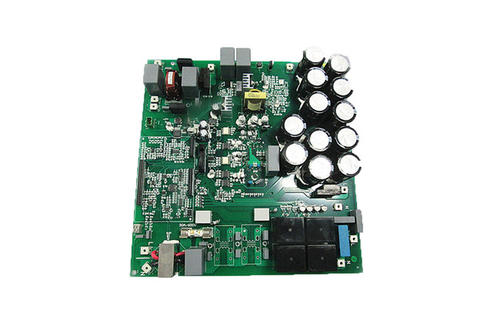
1. Power cord design: Based on the current of the sample circuit board, the power cord should be designed with a thicker width as much as possible, and the loop resistance should be appropriately reduced to ensure that the direction of the power cord and ground wire is consistent with the direction of data transmission. This design helps to enhance noise resistance. 2. Ground wire design: Digital ground and analog ground should be designed separately. If there are both logical and linear circuits on the circuit board, they should be separated as much as possible during design. Even for low-frequency circuits, single point parallel grounding should be used as much as possible. When there are difficulties in actual wiring, partial series connection can be used before parallel connection to ground. High frequency circuit boards should be grounded in series with multiple points, and the grounding wire should be short and leased. Grid shaped large area grounding foil should be used aro
Inquiry Now

