 +86 755 2794 4155
  sales@knownpcb.com
-
Shenzhen KNOWNPCB Technology Co., Ltd.
 +86 755 2794 4155
  sales@knownpcb.com
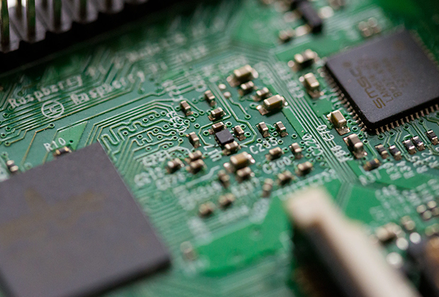
Have you noticed that now more and more of our lighting is using led lighting.What is LED? Compared to the traditional light bulbs, LEDs have lower power consumption, longer lifetime and higher energy efficiency. In the PCB industry,when we say LED PCB, it refers to the pcb used for LED lighting, if you are looking for a suitable LED PCB for your lighting system, this article may bring you something. WHAT ARE LEDS COMPOSED OF?LED is an initial light-emitting diode that produces light when an electric current passes through. LEDs typically have negative and positive electrodes, which generate light in the visible light region.The LEDS are glued to the PCB by soldering process and have electrical connections for lighting.Since light-emitting diodes dissipate a lot of heat when they are in use, when you are designing LED, the metal core is usually the best choice for LED PCB, it is because that it dissipates heat more faster. Among them, the metal material aluminum is the most widely used
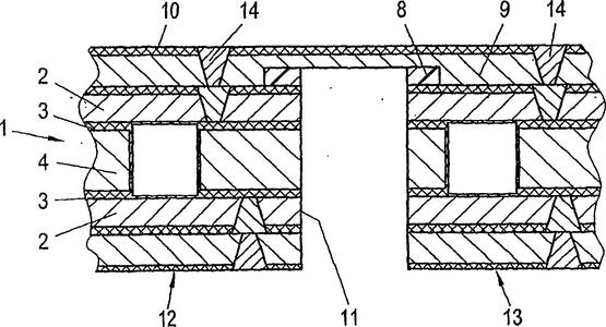
1、 Dry film mask with perforation Many customers believe that after a hole is broken, the film temperature and pressure should be increased to enhance its adhesion. However, this view is not correct because the solvent in the corrosion resistant layer evaporates excessively when the temperature and pressure are too high, making the dry film brittle and thin, making it easy to break through during development. We always need to maintain the toughness of the dry film. Therefore, after a hole is broken, we can improve it from the following points: 1. Reduce film temperature and pressure 2. Improve drilling edge 3. Increase exposure energy 4. Reduce development pressure 5. After applying the film, the parking time should not be too long to avoid causing the semi fluid like drug film at the corner to diffuse and thin under pressure 6. During the film application process, do not tension the dry film too tightly 2、 Penetration occurs during dry film electroplating The reason for

a) Ma Keng: Ma Keng is the result of organic pollution. A large pit usually indicates oil pollution. If the stirring is poor, the bubbles cannot be expelled, which will form pits. Wetting agents can be used to reduce its impact. We usually refer to small pitting as pinholes. Poor pre-treatment, metallic impurities, low boric acid content, and low plating temperature can all cause pinholes. Maintenance and process control of the plating solution are crucial, and anti pinhole agents should be used as process stabilizers to supplement. b) Roughness and burrs: Roughness indicates that the solution is dirty, which can be corrected by sufficient filtration (high pH can easily form hydroxide precipitates and should be controlled). If the current density is too high, impurities are brought in by impure anode mud and added water, and in severe cases, roughness and burrs will be produced. c) Low adhesion: If the copper coating is not fully oxidized, the coating will peel off and the adhesi
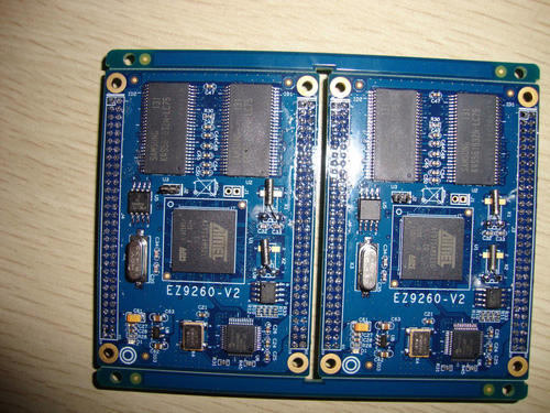
Conducting hole (VIA) is a common type of hole used to conduct or connect copper foil circuits between conductive patterns in different layers of a circuit board. For example, blind holes or buried holes, but cannot be inserted into copper plated holes of component leads or other reinforcement materials. Because PCBs are formed by stacking and accumulating many layers of copper foil, an insulation layer is laid between each layer of copper foil, so the copper foil layers cannot communicate with each other, and their signal connections rely on through holes (via), hence the Chinese name for through holes. The characteristic is that in order to meet the needs of customers, the conductive holes on the circuit board need to be plugged. This changes the traditional aluminum sheet plugging process by using white mesh to complete the circuit board surface solder mask and plug holes, making it stable in production, reliable in quality, and more perfect in use. Conducting holes mainly serv
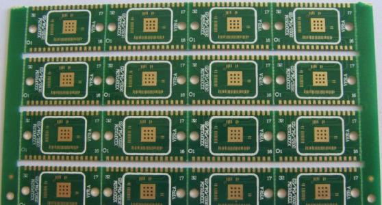
First, it is equal length. When designing a differential line, pay attention to making the lengths of the two signal lines the same. Because the length of the signal lines is the same, the transmission time of the signals is also the same, so the polarities of the differential signals will be different, resulting in the opposite situation. If the differential signal is the same, the signal quality will be poor.Next, is the isometric. That is to say, the distance between pairs of differential lines should be consistent. By adjusting the distance of the differential line, we can adjust a differential impedance in the whole process. What is the benefit of doing this? If our differential impedance can maintain a certain continuity, then there will be very few reflections and the transmitted signal will be very complete.Finally, it is the stacking of differential lines and printed boards. It is generally believed that the differential line will provide a reflow path for the printed board, a
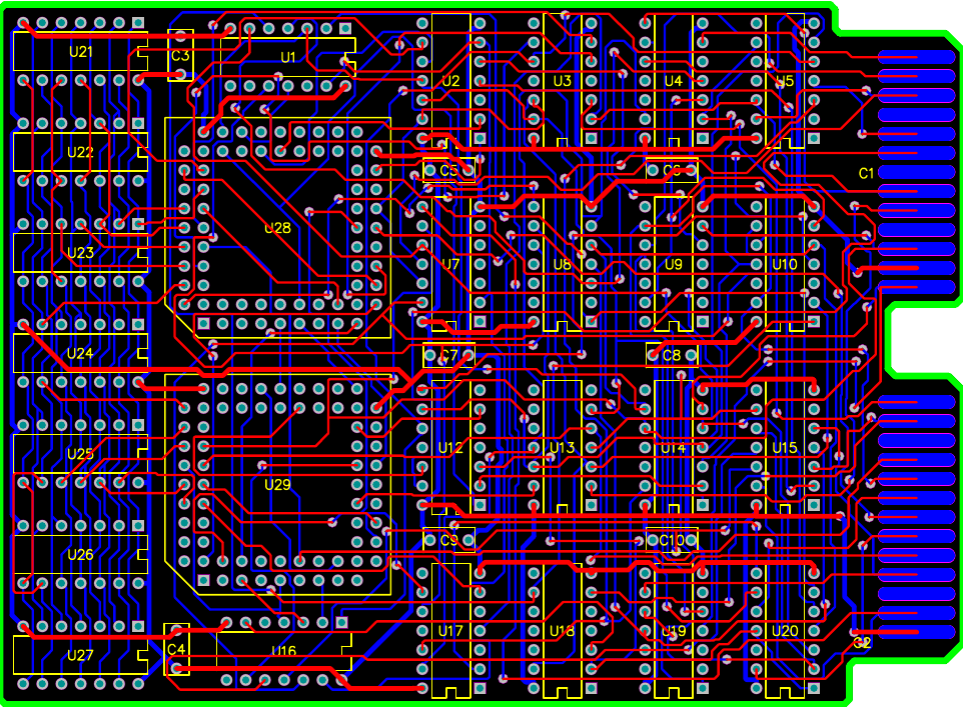
First, it is equal length. When designing a differential line, pay attention to making the lengths of the two signal lines the same. Because the length of the signal lines is the same, the transmission time of the signals is also the same, so the polarities of the differential signals will be different, resulting in the opposite situation. If the differential signal is the same, the signal quality will be poor. Next, is the isometric. That is to say, the distance between pairs of differential lines should be consistent. By adjusting the distance of the differential line, we can adjust a differential impedance in the whole process. What is the benefit of doing this? If our differential impedance can maintain a certain continuity, then there will be very few reflections and the transmitted signal will be very complete. Finally, it is the stacking of differential lines and printed boards. It is generally believed that the differential line will provide a reflow path for the printed
1. Report the results of the work The leader who lifts the heavy weight is the favorite. When reporting work, please remember to report the result to the leader first, and the result thinking is the first thinking. 2. Ask for work plan Please ensure that at least two programs are given to leaders, and express their views and effective suggestions. Don't let the leader do the quiz questions, but let the leader do the multiple-choice questions. Don't ask the leader how to do this thing, what to do, but ask, I have a plan, you can listen to it and see how it goes! 3. Summarize the work process and find three points To do a work summary, it is necessary to describe the process, not only to have a clear sequence and logic, but also to find out the key points, mistakes, and reflection points in the process. 4. Arrange work standards and clarify customer requirements Layout work must be clear about customer requirements and quality standards, otherwise subordinates will not know ho
After the customer's plug-in test, it is found that the via hole (via hole) is not connected. The test can be carried out normally before the plug-in, and the appearance has no drilling deviation phenomenon, which is mainly caused by the following five reasons: First: the hole copper is not enough; Second: the roughness of the hole wall is too large Third: Drilling dust plug holes Fourth: drilling broken knife to make up holes Fifth: poor solder mask plug hole In terms of controlling the problem of through-hole failure, the hole copper is the most important link. The automatic sinking copper line of our Honglian circuit is not small: Detection: The detection method of immersion copper wire is mainly backlight series detection. The number of series is more than 9 to be qualified to ensure the quality of copper immersion and hole formation. The detection methods include deposition speed force detection (copper layer thickness in standard time); glue removal speed force (this

One, circuit board factory tin surface quality defects So what are the factors that cause the bad tin surface of the tin surface? According to the analysis of the editor, there are the following points 1. The operation is not in accordance with the operating specifications when shipping The circuit industry has extremely strict requirements on the workshop environment and the standard operation of employees, especially the chemical reaction environment is required in the circuit board production process, so the infiltration of impurities is not allowed. After the board spraying process is completed, the subsequent one All series require employees to wear anti-static gloves to operate, because finger sweat or stains directly contact the surface, which will cause surface oxidation. If it causes defects, it is extremely difficult to find, and it is irregular, and it is difficult to be exposed in testing and tinning experiments. 2. The tin furnace for spraying tin is not cleaned on
Inquiry Now

