 +86 755 2794 4155
  sales@knownpcb.com
-
Shenzhen KNOWNPCB Technology Co., Ltd.
 +86 755 2794 4155
  sales@knownpcb.com
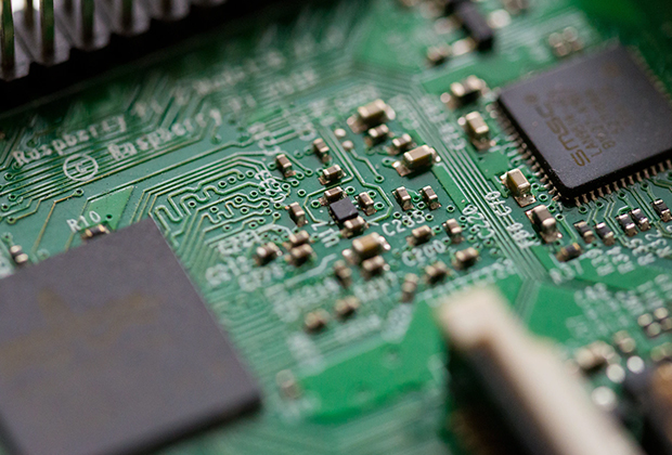
Have you noticed that now more and more of our lighting is using led lighting.What is LED? Compared to the traditional light bulbs, LEDs have lower power consumption, longer lifetime and higher energy efficiency. In the PCB industry,when we say LED PCB, it refers to the pcb used for LED lighting, if you are looking for a suitable LED PCB for your lighting system, this article may bring you something. WHAT ARE LEDS COMPOSED OF?LED is an initial light-emitting diode that produces light when an electric current passes through. LEDs typically have negative and positive electrodes, which generate light in the visible light region.The LEDS are glued to the PCB by soldering process and have electrical connections for lighting.Since light-emitting diodes dissipate a lot of heat when they are in use, when you are designing LED, the metal core is usually the best choice for LED PCB, it is because that it dissipates heat more faster. Among them, the metal material aluminum is the most widely used
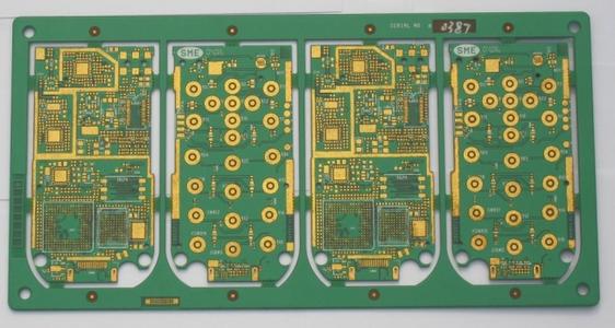
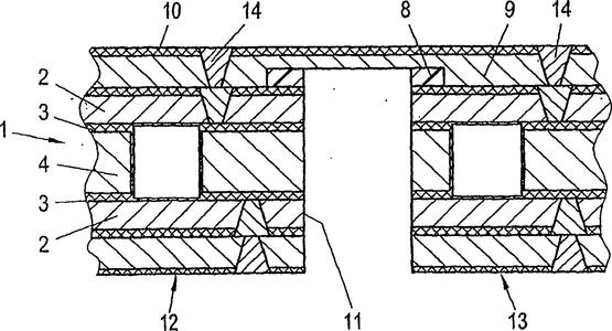
1. Process half of the hole with a double V-shaped cutting tool. 2. Second drill adds support holes at the edge of the hole, removes copper skin in advance, reduces burrs, and uses slot cutters to produce the drill, optimizing the speed and falling speed. 3. Copper plating is applied to the substrate by depositing a layer of copper on the hole wall of the circular holes on the edge of the board. 4. After laminating, exposing, and developing the outer circuit, the substrate is subjected to secondary copper plating and tin plating to thicken the copper layer on the hole wall of the circular hole at the edge of the board and cover it with a tin layer with anti-corrosion properties; 5. Half hole forming involves cutting the circular holes on the edge of the board in half to form a half hole; 6. Remove the anti electroplating film pressed during the process of film removal and pressing; 7. Etching is performed on the substrate to remove the exposed copper on the outer layer of the
a) Ma Keng: Ma Keng is the result of organic pollution. A large pit usually indicates oil pollution. If the stirring is poor, the bubbles cannot be expelled, which will form pits. Wetting agents can be used to reduce its impact. We usually refer to small pitting as pinholes. Poor pre-treatment, metallic impurities, low boric acid content, and low plating temperature can all cause pinholes. Maintenance and process control of the plating solution are crucial, and anti pinhole agents should be used as process stabilizers to supplement. b) Roughness and burrs: Roughness indicates that the solution is dirty, which can be corrected by sufficient filtration (high pH can easily form hydroxide precipitates and should be controlled). If the current density is too high, impurities are brought in by impure anode mud and added water, and in severe cases, roughness and burrs will be produced. c) Low adhesion: If the copper coating is not fully oxidized, the coating will peel off and the adhesi
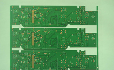
1、 Dry film mask with perforation Many customers believe that after a hole is broken, the film temperature and pressure should be increased to enhance its adhesion. However, this view is not correct because the solvent in the corrosion resistant layer evaporates excessively when the temperature and pressure are too high, making the dry film brittle and thin, making it easy to break through during development. We always need to maintain the toughness of the dry film. Therefore, after a hole is broken, we can improve it from the following points: 1. Reduce film temperature and pressure 2. Improve drilling edge 3. Increase exposure energy 4. Reduce development pressure 5. After applying the film, the parking time should not be too long to avoid causing the semi fluid like drug film at the corner to diffuse and thin under pressure 6. During the film application process, do not tension the dry film too tightly 2、 Penetration occurs during dry film electroplating The reason for
In terms of electrical performance, it includes dielectric constant and loss angle, ① dielectric constant or dielectric coefficient, and the surface is a coefficient of insulation capacity characteristics, measured in units of ε In actual production, the dielectric constant is not an absolute value, but expressed in the form of relative dielectric constant The loss angle, also known as the "loss factor" or "damping factor", is the tangent of the phase difference angle between the strain and stress cycles of a material in the residual alternating field, which is also equal to the ratio of the loss film amount of the material to the stored energy modulus. Thermal performance method: It is necessary to have a certain understanding of the relevant characteristic parameters. Below, we will introduce the definition manual of thermal performance parameters for two different sheet materials: ① From the perspective of board types alone, it can be mainly divided into Tg value, Td value, CT
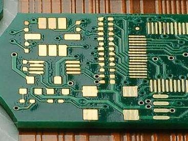
① Inner layer production: Multilayer circuit boards are made by pressing two or more double-sided boards. For some high-frequency multi-layer boards, the inner layer holes may be blind holes, and the inner layer boards need to be drilled and then pressed together. ② Drilling: Based on the production capacity of the factory, verify the data. If the line width moment or aperture is less than the manufacturing capacity, the engineering department should improve communication with the customer and reach a consensus to compensate for a certain stroke of the line width moment or aperture. Generally, the drilling roughness is controlled at ≤ 25.4um. ③ Copper plating: Usually, during transportation or production, there may be scratches on the substrate copper foil, causing it to be exposed to the surface. It is necessary to go through processes such as copper plating to ensure that the thickness of the PCB board copper foil meets the customer's order requirements. Secondly, according to

1. IPC/EIA/JEDECJ-STD-003A: Solderability testing for customized circuit boards. 2. IPC-6018A: Manufacturing inspection and testing of microwave finished circuit boards, including manufacturing performance and qualification requirements for high-frequency circuit boards. 3. IPC-M-103: Surface Mount Assembly Manual Standard, which includes all 21 IPC documents related to PCB surface mount. 4. IPC-M-I04: PCB Manufacturing and Assembly Manual Standard, which includes the 10 most widely used documents related to circuit board manufacturing and assembly. 5. IPC-DRM-53: Introduction to Electronic PCB Assembly Desktop Reference Manual, with illustrations and photos describing through-hole installation and surface mount assembly techniques. 6. IPC-Ca-821: General requirements for thermal conductive adhesives, including requirements and testing methods for thermal conductive dielectrics that bond components to appropriate positions. 7. IPC-3406: Guidelines for Conductive Surface Coati
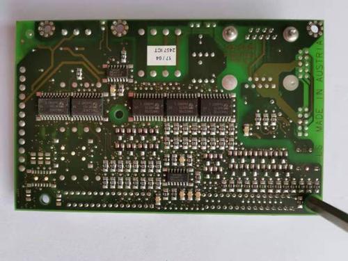
During the production process of PCB circuit boards, it is common to encounter poor copper wire detachment, also known as copper throwing, which affects product quality. So, what are the common reasons for PCB circuit board copper throwing? 1、 PCB process factors: 1. Copper foil is excessively etched, and the electrolytic copper foil used in the market is generally single-sided galvanized (commonly known as ashed foil) and single-sided copper plating (commonly known as reddened foil). The common copper throwing is generally ashed foil above 70um, while reddened foil and ashed foil below 18um have not undergone bulk copper throwing. 2. Local collisions occurred during the PCB process, causing the copper wire to detach from the substrate due to external mechanical forces. This defect manifests as poor positioning or directionality, where the detached copper wire will have obvious twisting or scratches/impact marks in the same direction. 3. Unreasonable PCB circuit design, using t
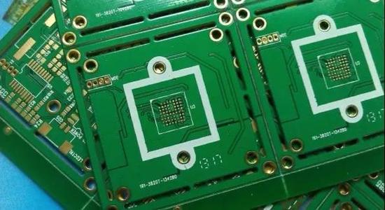
Aluminum substrate is a unique metal based copper clad plate with good thermal conductivity, electrical insulation performance, and mechanical processing performance. Let the aluminum substrate manufacturer provide you with a detailed explanation of the aluminum substrate. 1、 Characteristics of aluminum substrate 1. Adopting Surface Mount Technology (SMT); 2. Effectively handle thermal diffusion in circuit design schemes; 3. Reduce product operating temperature, improve product power density and reliability, and extend product service life; 4. Reduce product volume, reduce hardware and assembly costs; 5. Replace fragile ceramic substrates for better mechanical durability. 2、 Structure of aluminum substrate Aluminum based copper clad plate is a metal circuit board material composed of copper foil, thermal insulation layer, and metal substrate: Copper foil: equivalent to a copper clad board of a regular PCB, with a copper foil thickness of loz to 10oz for the circuit. Therm
Inquiry Now

