 +86 755 2794 4155
  sales@knownpcb.com
-
Shenzhen KNOWNPCB Technology Co., Ltd.
 +86 755 2794 4155
  sales@knownpcb.com
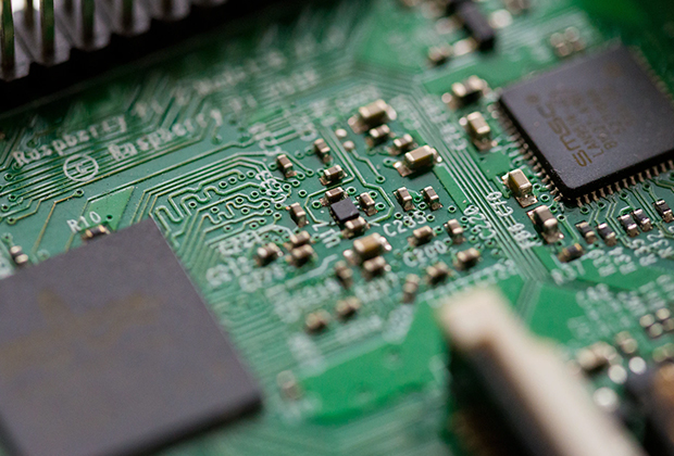
Have you noticed that now more and more of our lighting is using led lighting.What is LED? Compared to the traditional light bulbs, LEDs have lower power consumption, longer lifetime and higher energy efficiency. In the PCB industry,when we say LED PCB, it refers to the pcb used for LED lighting, if you are looking for a suitable LED PCB for your lighting system, this article may bring you something. WHAT ARE LEDS COMPOSED OF?LED is an initial light-emitting diode that produces light when an electric current passes through. LEDs typically have negative and positive electrodes, which generate light in the visible light region.The LEDS are glued to the PCB by soldering process and have electrical connections for lighting.Since light-emitting diodes dissipate a lot of heat when they are in use, when you are designing LED, the metal core is usually the best choice for LED PCB, it is because that it dissipates heat more faster. Among them, the metal material aluminum is the most widely used
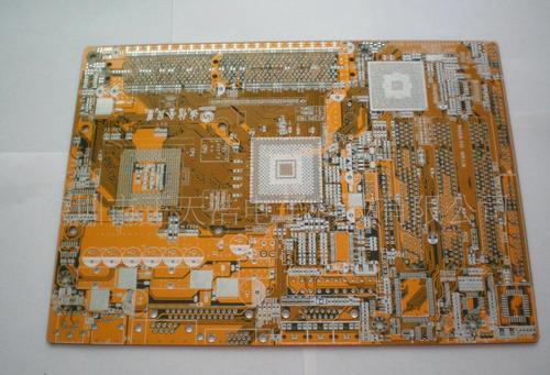
The main purpose of vacuum aluminum coating film is to replace pure aluminum foil composite, giving soft packaging printed materials an elegant silver white luster, and reducing packaging printing costs while improving the barrier and shading properties of soft packaging film bags (aluminum coating film instrument is 0.4~0.6) μ m. Only about 1/150) 25% of the amount of pure aluminum foil used. The PCB sampling manufacturer tells you that there are two common vacuum aluminum plating methods: One is vacuum aluminum plating after printing, which involves reverse inner printing on the surface of the thin film, followed by aluminum plating, and then composite with the bottom film; The second is to directly imprint on the surface of the thin film, and then dry composite it with the vacuum aluminum plated bottom film. But this method requires the use of materials such as CPP and PE with good heat resistance and heat sealing for the bottom film. No matter what method is used, the compo
1. Industry regulatory authorities and regulatory system The Ministry of Industry and Information Technology of China is the competent department in charge of the printed circuit board industry. Its main responsibilities include formulating and organizing the implementation of industry plans, plans, and policies for the industrial and communication industries, proposing policy recommendations for optimizing industrial layout and structure, drafting relevant laws and regulations, formulating regulations, drafting industry technical specifications and standards, and organizing their implementation, guiding industry quality management work. The Electronic Information Department under the Ministry of Industry and Information Technology of China is responsible for industry management of electronic information product manufacturing; Organize and coordinate the development and production of major system equipment, microelectronics and other basic products, and organize and coordinate the
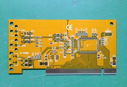
Negative film of circuit board: Generally speaking, it is the tenting process that uses acidic etching negative film because after the film is made, the desired circuit or copper surface is transparent, while the unwanted parts are black. After exposure by the circuit process, the transparent part hardens chemically due to the exposure of the dry film inhibitor to light. The subsequent development process will wash away the dry film that has not hardened, So in the etching process, only a portion of the copper foil (the black part of the film) that has been washed off by biting off the dry film is retained, while the circuit (the transparent part of the film) that belongs to our desired circuit (PCB sample) is retained. We will tell you about the positive of the circuit board. Generally, this is the pattern process we are talking about, and the solution used is alkaline etching positive. If viewed from the negative, the desired circuit or copper surface is black, while the other pa
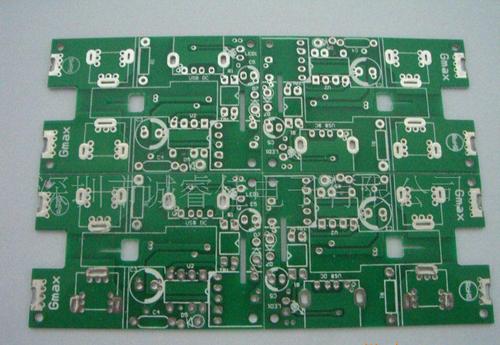
The earlier the signal integrity (SI) problem is solved, the higher the efficiency of the design, which can avoid adding termination devices only after the circuit board design is completed. There are many tools and resources available for SI design planning. This article explores the core issues of signal integrity and several methods to solve SI problems, ignoring the technical details of the design process. With the increase of IC output switching speed, almost all designs have encountered signal integrity issues regardless of the signal cycle. Even if you haven't encountered SI issues in the past, as the working frequency of the circuit increases, you will definitely encounter signal integrity issues in the future. The signal integrity problem mainly refers to the phenomenon of signal overshoot and damping oscillation, which are mainly functions of IC driving amplitude and jump time. That is to say, even if the wiring topology remains unchanged, as long as the chip speed beco
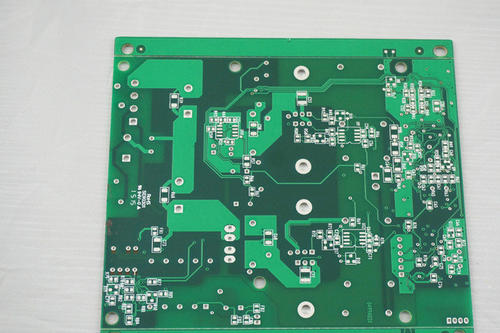
1. Engineering design: Precautions for printed circuit board design: A. The arrangement of interlayer semi cured sheets should be symmetrical, for example, for a six layer board, the thickness and number of semi cured sheets between layers 1-2 and 5-6 should be consistent, otherwise it is easy to warp after lamination. B. Multi layer core boards and semi cured sheets should use products from the same supplier. C. The area of the circuit diagram on the outer A and B sides should be as close as possible. If side A is a large copper surface and side B only runs a few wires, this type of printed circuit board is prone to warping after etching. If the area difference between the two sides of the circuit is too large, independent grids can be added to the sparse side for balance. 2. Drying board before cutting: The purpose of drying the copper-clad board before cutting (150 degrees Celsius, time 8 ± 2 hours) is to remove moisture from the board and completely cure the resin inside t
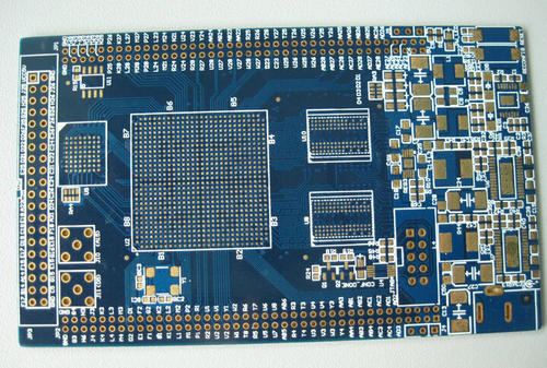
1、 Why do circuit boards require a very flat surface The circuit board prototype manufacturer tells you that if the printed circuit board is not flat on the automated insertion line, it will cause inaccurate positioning, prevent components from being inserted into the holes and surface mounting pads of the board, and even damage the automatic insertion machine. The board where the components are installed is bent after welding, making it difficult to cut the component legs flat and neat. The board cannot be installed on the chassis or socket inside the machine, so it is also very troublesome for the assembly plant to encounter board warping. At present, printed boards have entered the era of surface installation and chip installation, and assembly plants are bound to have increasingly strict requirements for board warping. 2、 Standards and testing methods for warpage According to the American IPC-6012 (1996 edition), the allowable large warpage and distortion for surface mount
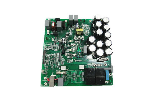
The positioning of CNC milling is to use positioning pins to position the printed circuit board to be processed on the workbench of the milling machine, so as to conveniently and accurately process the shape of the printed circuit board. Require simple and reliable positioning, capable of quickly loading and unloading boards while eliminating chips. The manufacturer of circuit board samples tells you that there are various positioning methods, such as the design of reciprocating workbenches for some milling machines. When one worktable is being processed, the other worktable loads and unloads the board. There is also a method of using two sets of milling positioning pads. When one milling positioning pad is processed on the CNC milling workbench, the other milling positioning pad is loaded and unloaded on the platform. The exchange between the two only takes a few seconds. The CNC milling worktable itself is a positioning plate, which is an aluminum alloy plate fixed with pins and
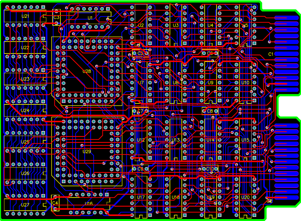
In circuit design, we are generally concerned about signal quality issues, but sometimes we limit our research to signal lines and treat power and ground as ideal situations. Although this approach can simplify the problem, it is no longer feasible in high-speed design. Although the direct result of circuit design is reflected in signal integrity, we cannot ignore power integrity design as a result. Because the integrity of the power supply directly affects the signal integrity of the subsequent PCB board. Power integrity and signal integrity are closely related, and in many cases, PCB sample manufacturers believe that the main cause of signal distortion is the power system. For example, excessive ground rebound noise, inappropriate design of decoupling capacitors, severe circuit impact, poor separation of multiple power sources/ground planes, unreasonable geological design, uneven current, and so on. 1) Power distribution system Power integrity design is a very complex task, but i
Inquiry Now

