 +86 755 2794 4155
  sales@knownpcb.com
-
Shenzhen KNOWNPCB Technology Co., Ltd.
 +86 755 2794 4155
  sales@knownpcb.com
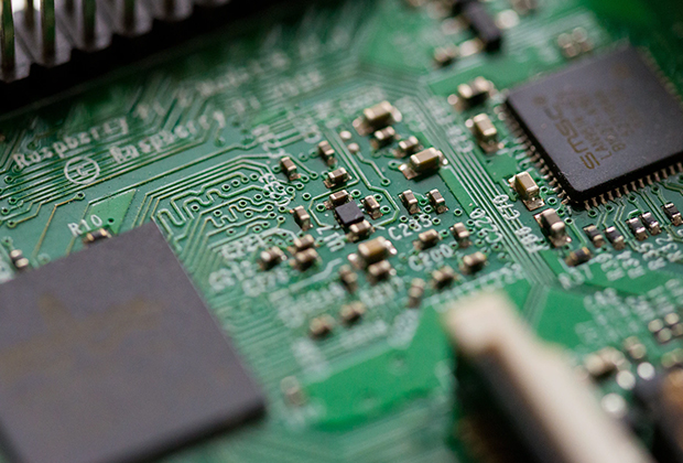
Have you noticed that now more and more of our lighting is using led lighting.What is LED? Compared to the traditional light bulbs, LEDs have lower power consumption, longer lifetime and higher energy efficiency. In the PCB industry,when we say LED PCB, it refers to the pcb used for LED lighting, if you are looking for a suitable LED PCB for your lighting system, this article may bring you something. WHAT ARE LEDS COMPOSED OF?LED is an initial light-emitting diode that produces light when an electric current passes through. LEDs typically have negative and positive electrodes, which generate light in the visible light region.The LEDS are glued to the PCB by soldering process and have electrical connections for lighting.Since light-emitting diodes dissipate a lot of heat when they are in use, when you are designing LED, the metal core is usually the best choice for LED PCB, it is because that it dissipates heat more faster. Among them, the metal material aluminum is the most widely used
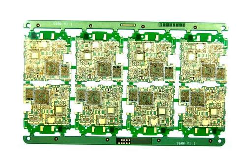
Key components require preset test points on the PCB circuit board. The solder pads used for welding appearance assembly components are not allowed to be used as inspection points. A dedicated test solder pad must be pre-set to ensure smooth solder joint inspection and production debugging. The solder pads used for testing should be arranged on the unified side of the PCB circuit board as much as possible, which is beneficial for testing and reduces the cost of testing. The following circuit board sample manufacturer will tell you its process preset requirements: (1) The distance between test points and the edge of the PCB circuit board should be greater than 5mm; (2) The test point should not be covered by solder mask or text ink; (3) The testing point should be preferably coated with solder or selected with a soft, easy to penetrate, and non oxidizing metal to ensure reliable grounding and extend the service life of the probe (4) The testing point should be placed 1mm away fr
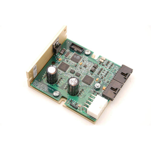
PCBA test stand is a device used to test PCBA finished products. When making PCBA test racks, PCBA processing plants usually need to provide Gerber files and PCBA samples to facilitate the production of test racks. For the current PCBA test bench, only a few pressure plate buckles are installed on the test bench, and the PCBA is fixed by a thimble and pressure plate buckle. During the PCBA function test, press the PCBA into the pressure plate buckle with both hands. Due to uneven force or insufficient compression, PCBA can easily cause poor contact between the testing needle and PCBA, seriously affecting testing efficiency and accuracy; If too much force is applied, it is easy to deform or damage the PCBA when pressing down, and it is also easy to damage the test needle of the testing frame, causing significant losses. 1、 Material preparation After determining the plan based on the information, it is necessary to prepare hardware materials (electronic components), relevant additi
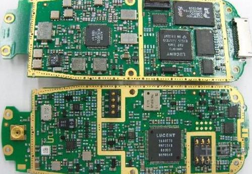
Aluminum substrate is a unique metal based copper clad plate with good thermal conductivity, electrical insulation performance, and mechanical processing performance. Let the aluminum substrate manufacturer provide you with a detailed explanation of the aluminum substrate. 1、 Characteristics of aluminum substrate 1. Adopting Surface Mount Technology (SMT); 2. Effectively handle thermal diffusion in circuit design schemes; 3. Reduce product operating temperature, improve product power density and reliability, and extend product service life; 4. Reduce product volume, reduce hardware and assembly costs; 5. Replace fragile ceramic substrates for better mechanical durability. 2、 Structure of aluminum substrate Aluminum based copper clad plate is a metal circuit board material composed of copper foil, thermal insulation layer, and metal substrate: Copper foil: equivalent to a copper clad board of a regular PCB, with a copper foil thickness of loz to 10oz for the circuit. Therm
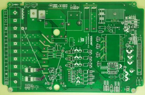
1. If the PCB has a large amount of ground, such as SGND, AGND, GND, etc., it is necessary to use the most important "ground" as the reference for independent copper coating based on the different positions of the PCB surface. Separate the digital and analog power lines for copper coating, and before copper coating, thicken the corresponding power lines: 5.0V, 3.3V, etc. 2. For single point connections to different locations, the method is to connect through a 0 ohm resistor, magnetic bead, or inductor. 3. The crystal oscillator in the circuit is a high-frequency emission source. For the copper coating near the crystal oscillator, the method is to surround the crystal oscillator with copper coating, and then ground the outer shell of the crystal oscillator separately. 4. If the problem of islands (dead zones) is significant, then define a place and add it through a hole. 5. When starting wiring, the ground wire should be treated equally. When wiring, the ground wire should be pro
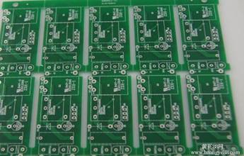
During the production process of PCB circuit boards, it is common to encounter poor copper wire detachment, also known as copper throwing, which affects product quality. So, what are the common reasons for PCB circuit board copper throwing? 1、 PCB process factors: 1. Copper foil is excessively etched, and the electrolytic copper foil used in the market is generally single-sided galvanized (commonly known as ashed foil) and single-sided copper plating (commonly known as reddened foil). The common copper throwing is generally ashed foil above 70um, while reddened foil and ashed foil below 18um have not undergone bulk copper throwing. 2. Local collisions occurred during the PCB process, causing the copper wire to detach from the substrate due to external mechanical forces. This defect manifests as poor positioning or directionality, where the detached copper wire will have obvious twisting or scratches/impact marks in the same direction. 3. Unreasonable PCB circuit design, using t

The so-called copper coating of PCB circuit boards refers to using the idle space on the PCB as a reference plane, and then filling it with solid copper. These copper areas are also known as copper filling. The significance of copper coating is to reduce the impedance of the ground wire and improve its anti-interference ability; Reduce voltage drop and improve power efficiency; Connecting to the ground wire can also reduce the loop area. There are generally two methods of copper coating, namely large-scale copper coating and grid copper coating. Large area copper coating has the dual functions of increasing current and shielding, but if the copper coating is applied on a large area, the board may curl up and even bubble during wave soldering. Therefore, when covering a large area with copper, several grooves are usually opened to alleviate blistering on the copper foil. Grid copper coating, from the perspective of heat dissipation, reduces the heating surface of copper and plays a
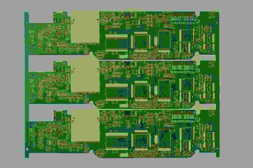
Electrical principles and mechanical structure design, determining the size and structural shape of the PCB based on the overall structure of the machine. Draw a process diagram of the SMT printed circuit board, indicating the length, width, and thickness of the PCB, the position and size of structural components and assembly holes, and leaving edge dimensions, so that circuit designers can carry out wiring design within an effective range. The choice of assembly form depends on the type of components in the circuit, the size of the circuit board, and the equipment conditions of the production line. PCB board sampling shares with you the principles for selecting the assembly form of printed boards: following the principles of optimizing processes, reducing costs, and improving product quality, first determine the overall goals of electronic product functions, performance indicators, costs, and overall dimensions of the entire machine. When developing and designing new products, th
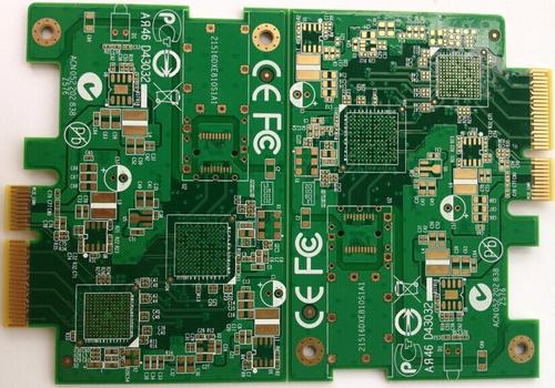
Pre impregnated material is a sheet-like material composed of resin and carrier. Among them, the resin is in the B-stage, under the action of temperature and pressure, it has fluidity and can quickly cure and complete the bonding process, and together with the carrier, forms an insulation layer. Commonly known as semi cured sheet or adhesive sheet. To ensure the high reliability and quality stability of multi-layer printed circuit boards, it is necessary to conduct quality testing on the characteristics of semi-solid chips (test layer pressing method). The characteristics of electroplating semi cured chips on circuit boards include two parts: pre lamination characteristics and post lamination characteristics. The characteristics before lamination mainly refer to: resin content%, fluidity%, volatile content% and gel time (S). The circuit board prototype manufacturer will share with you the characteristics after lamination, including electrical performance, thermal shock performance,
Inquiry Now

