 +86 755 2794 4155
  sales@knownpcb.com
-
Shenzhen KNOWNPCB Technology Co., Ltd.
 +86 755 2794 4155
  sales@knownpcb.com
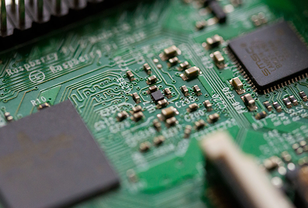
Have you noticed that now more and more of our lighting is using led lighting.What is LED? Compared to the traditional light bulbs, LEDs have lower power consumption, longer lifetime and higher energy efficiency. In the PCB industry,when we say LED PCB, it refers to the pcb used for LED lighting, if you are looking for a suitable LED PCB for your lighting system, this article may bring you something. WHAT ARE LEDS COMPOSED OF?LED is an initial light-emitting diode that produces light when an electric current passes through. LEDs typically have negative and positive electrodes, which generate light in the visible light region.The LEDS are glued to the PCB by soldering process and have electrical connections for lighting.Since light-emitting diodes dissipate a lot of heat when they are in use, when you are designing LED, the metal core is usually the best choice for LED PCB, it is because that it dissipates heat more faster. Among them, the metal material aluminum is the most widely used
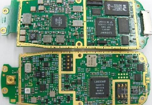
1、 PCB circuit board process elements: 1. Excessive etching of copper foil. The electrolytic copper foil used in the market is generally single-sided galvanized (commonly known as ashing foil) and single-sided copper plating (commonly known as reddening foil). The common copper throwing is generally galvanized copper foil with a thickness of 70um or more, while reddening foil and ashing foil with a thickness of 18um or less have not shown batch copper throwing. 2. During the PCB process, local collisions occurred, causing the copper wire to detach from the substrate due to external mechanical forces. This defect manifests as poor positioning or directionality, with significant twisting of dropped copper wires or scratches/impact marks in the same direction. Peel off the defective copper wire and observe the rough surface of the copper foil. It can be seen that the color of the rough surface of the copper foil is normal, and there will be no side corrosion defects. The peeling stre
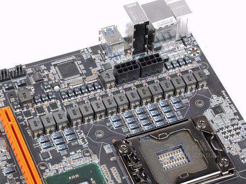
The update and iteration of electronic products are relatively fast, and the development efforts are also increasing. The demand for PCB board making is also gradually growing, and the market share is constantly expanding. With the increasing process requirements and information speed of electronic products, PCB board making is rising rapidly. So, after designing the PCB, what are the relevant parameters and explanations of demand and supply when outsourcing the PCB? Below, the editor will explain them in detail. Relevant parameters and clarification of PCB sample demand and supply 1. Information: The first thing to clarify is what kind of PCB manufacturing materials are required. Currently, the most common one is using FR4, and the main information is epoxy resin peeled fiber cloth board. 2. Board layer: To clarify the number of layers you use to make a PCB. 3. Is it a single piece shipment or a demand for panel shipment? If panel shipment is required, the number of panels nee
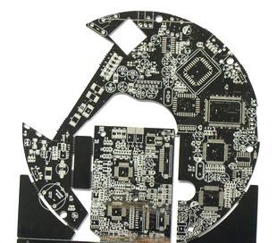
1. The thickness of the board is 0.8, 1.0, 1.2, 1.6, 2.0, which are commonly used specifications. If there are no special requirements, choose a board thickness of 1.6mm. 2. Copper foil thickness: 0.5, 1.0, 2.0 are commonly used specifications. If the power is not particularly high, it is not necessary to choose a board. Manufacturers usually use a board with a power of 0.5oz. If the power is around 100W, a board with a power of 1.0 or above will be used. 3. The colors for solder mask: green, black, red, and white are commonly used. If there are no specific requirements, green should be used. If you are using it for your own experiment, you should use green even more because this color is the clearest for circuit boards. 4. Solder pad treatment: sinking gold, anti oxidation, tin spraying (divided into lead and lead-free), generally choose the latter two, and the preservation time of tin spraying will be longer. 5. Screen printing colors: White and black are commonly used colo
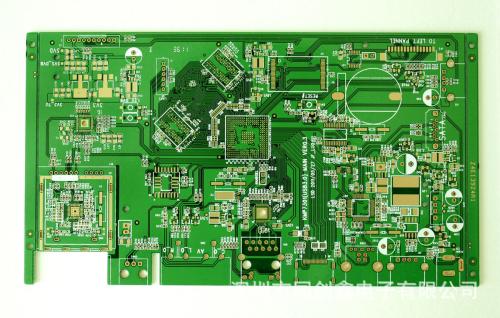
The volume of electronic products is becoming increasingly thin and short, and directly stacking holes on through blind holes is a design method to achieve high-density interconnection. To do a good job of stacking holes, the first step is to ensure the flatness of the hole bottom. There are several production methods, and the electroplating hole filling process is one of the representative ones. Next, let the PCB engineer teach you about the PCB electroplating hole filling process. 1. Advantages of electroplated hole filling: (1) Beneficial for designing stacked holes and holes on the disc; (2) Improving electrical performance helps with high-frequency design; (3) Helps to dissipate heat; (4) Plug holes and electrical interconnections are completed in one step; (5) The blind hole is filled with electroplated copper, which has higher reliability and better conductivity than conductive adhesive. 2. Physical impact parameters The physical parameters that need to be studied in
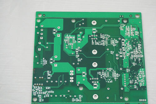
Dry film is a polymer material that can block electroplating and etching functions. Its reaction principle is to polymerize through ultraviolet radiation, producing stable substances attached to the board surface. It is a widely used consumer material in the microelectronics industry and circuit board manufacturing industry. Today, the editor of CITIC China PCB will talk to you about the types of PCB dry films. 1. Single sided PCB The substrate material is mainly composed of paper phenol copper laminated board (paper phenol as the bottom, covered with copper foil) and paper epoxy resin copper laminated board. Most of them are used in household appliances such as radios, AV appliances, heaters, refrigerators, washing machines, as well as commercial machines such as printers, vending machines, circuit breakers, and electronic components, with the advantage of low prices. 2. Double sided PCB The substrate material is mainly Glass-Epoxy copper laminated board, GlassComposite (glass

In order to save production costs, almost every PCB factory performs panel assembly operations before orders enter the workshop. Splicing boards is not just about putting various small boards together into one big board, but there are many things to pay attention to and important principles. Today, let the editor of Zhongxinhua summarize with everyone~ Firstly, there is the issue of splicing, and the reason for this is to save production costs. To avoid unnecessary waste, splicing treatment will be carried out before production on the circuit board production line without affecting the circuit board. For PCB panel width ≤ 260mm~300mm, it varies depending on the production line. Because we may have many materials and each material gun corresponds to a module in our own processing equipment, if the splicing exceeds the range of the module, the processing speed will become very slow. The outer frame (clamping edge) of the PCB panel should be carefully considered to ensure that the

Rigid flexible combination board is a method of laminating a flexible circuit substrate and a rigid circuit substrate together, which has both the rigidity of a hard board and the flexibility of a soft board. So, what issues should be paid attention to when making rigid flexible composite boards? 1. The design of rigid flexible composite plates usually changes from rigidity to flexibility, and then to rigidity. The rigid region generally has more layers than the flexible region, and the material is transferred from FR-4 to polyimide in the transition region. When intersection occurs, the overlap between rigid and flexible materials needs to keep the holes away from the transition area to maintain integrity. In addition, many rigid and flexible designs incorporate reinforcing materials such as stainless steel or aluminum to provide additional support for connectors and components. 2. Flexible circuits have bent wires that can affect wiring. Due to possible material stress, it is n
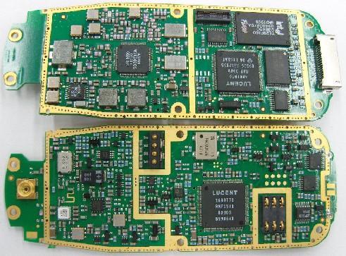
Industrial circuit board damage usually refers to a component being damaged, possibly a chip, a capacitor, or even a small resistor. The repair process involves identifying and replacing the damaged component. 1. Resistors with small resistance values and capacitors with large capacity are prone to damage A resistor with a small resistance value is often used in power supply lines to limit current, which acts as a fuse. If the current is too high, it will first burn out. In addition, many ground capacitors are used in power supply lines for filtering, and their size and capacity are generally large. If the voltage or current is unstable, the capacitors will break down and cause leakage. 2. Fault characteristics and maintenance of capacitor damage The failure caused by capacitor damage is the highest in electronic devices, with electrolytic capacitor damage being the most common. Capacitor damage is manifested as: 1. reduced capacity; 2. Complete loss of capacity; 3. Leakage; 4
Inquiry Now

