 +86 755 2794 4155
  sales@knownpcb.com
-
Shenzhen KNOWNPCB Technology Co., Ltd.
 +86 755 2794 4155
  sales@knownpcb.com
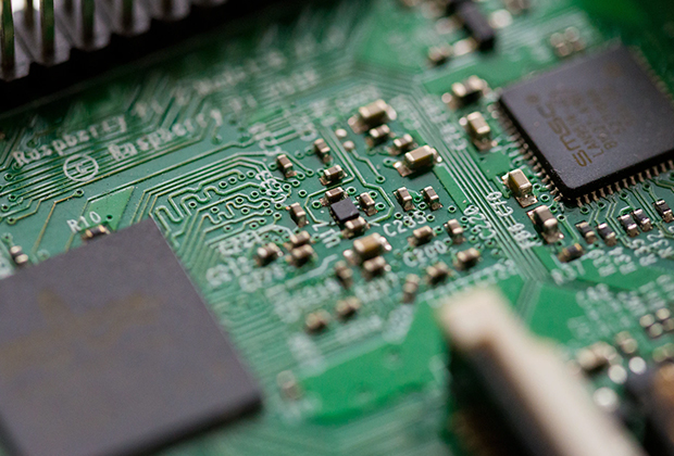
Have you noticed that now more and more of our lighting is using led lighting.What is LED? Compared to the traditional light bulbs, LEDs have lower power consumption, longer lifetime and higher energy efficiency. In the PCB industry,when we say LED PCB, it refers to the pcb used for LED lighting, if you are looking for a suitable LED PCB for your lighting system, this article may bring you something. WHAT ARE LEDS COMPOSED OF?LED is an initial light-emitting diode that produces light when an electric current passes through. LEDs typically have negative and positive electrodes, which generate light in the visible light region.The LEDS are glued to the PCB by soldering process and have electrical connections for lighting.Since light-emitting diodes dissipate a lot of heat when they are in use, when you are designing LED, the metal core is usually the best choice for LED PCB, it is because that it dissipates heat more faster. Among them, the metal material aluminum is the most widely used
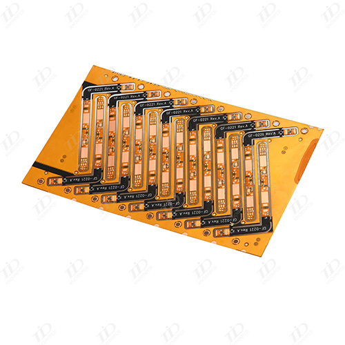
After using printed boards in electronic devices, due to the consistency of similar printed boards, errors in manual wiring are avoided, and electronic components can be automatically inserted or pasted, soldered, and inspected, ensuring the quality of electronic devices, improving labor productivity, reducing costs, and facilitating maintenance. Development: Printed circuit boards have evolved from single-layer to double-sided, multi-layer, and flexible, and still maintain their respective development trends. Due to the continuous development towards high precision, high density, and high reliability, as well as the reduction of volume, cost, and performance, printed circuit boards still maintain strong vitality in the future development of electronic equipment engineering. The discussion on the development trend of future printed circuit board production and manufacturing technology at home and abroad is basically consistent, which is to develop towards high-density, high-prec
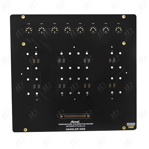
A printed board is better when installed upright, and the distance between boards should generally not be less than 2cm. Moreover, the arrangement of devices on the printed board should follow certain rules: For equipment that uses free convection air cooling, it is better to arrange integrated circuits (or other devices) in a longitudinal manner; For equipment that uses forced air cooling, it is better to arrange integrated circuits (or other devices) in a horizontal and elongated manner; Devices on the same printed circuit board should be arranged in zones according to their heat generation and heat dissipation degree as much as possible. Devices with low heat generation or poor heat resistance (such as small signal transistors, small-scale integrated circuits, electrolytic capacitors, etc.) should be placed upstream (at the inlet) of the cooling airflow, while devices with high heat generation or good heat resistance (such as power transistors, large-scale integrated circuits
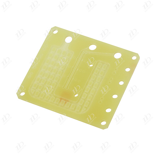
1. Component packaging (1) Pad spacing If it is a new device, you need to draw the component packaging yourself to ensure proper spacing, as the pad spacing directly affects the soldering of the component. (2) Through-hole size (if any) For plug-in devices, sufficient margin should be reserved for through-hole size, generally not less than 0.2mm is more appropriate. (3) Contour screen printing The contour screen of the device is slightly larger than its actual size, ensuring that the device can be installed smoothly. 2. PCB board layout (1) IC should not be placed near the board edge. (2) Components of the same module circuit should be placed close to each other For example, decoupling capacitors should be placed close to the power pins of the IC, and components that make up the same functional circuit should be prioritized and placed in one area with clear hierarchy to ensure the implementation of functions. (3) Arrange the position of sockets according to actual instal
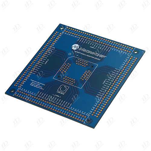
(1) Terminating resistor It is better to connect a matching resistor at the end of a high-speed line or a digital signal line with higher frequency and longer routing. (2) Connect the input signal line to a small capacitor in parallel It is better to connect the signal line input from the interface to a small capacitor at the interface level near the interface. The size of the capacitor is determined by the strength and frequency of the signal, and cannot be too large, otherwise it will affect the integrity of the signal. For low-speed input signals, such as button inputs, a 330pF small capacitor can be selected, as shown in Figure 2. Figure 2: PCB board design_ Connect the input signal line to a small capacitor Figure 2: PCB board design_ Connect the input signal line to a small capacitor (3) Driving ability For example, a switch signal with a high driving current can be driven by a transistor; For buses with large fan outs, buffer drivers can be added.

Electromagnetic compatibility refers to the ability of electronic devices to work in a coordinated and effective manner in various electromagnetic environments. The purpose of electromagnetic compatibility design is to enable electronic devices to suppress various external interferences, enabling them to operate normally in specific electromagnetic environments, while also reducing the electromagnetic interference of electronic devices themselves on other electronic devices. Choose a reasonable wire width. The impact interference generated by transient current on printed lines is mainly caused by the inductance component of printed wires, so the inductance of printed wires should be minimized as much as possible. The inductance of printed wires is directly proportional to their length and inversely proportional to their width, so short and precise wires are beneficial for suppressing interference. The signal lines of clock leads, row drivers, or bus drivers often carry large trans

Correctly selecting single point grounding and multi-point grounding in low-frequency circuits, where the operating frequency of the signal is less than 1MHz, the wiring and inductance between devices have less impact, while the circulating current formed by the grounding circuit has a greater impact on interference. Therefore, single point grounding should be used. When the operating frequency of the signal is greater than 10MHz, the impedance of the ground wire becomes large. At this time, the impedance of the ground wire should be reduced as much as possible, and nearby multi-point grounding should be used. When the working frequency is between 1-10MHz, if a single point grounding is used, the length of the ground wire should not exceed 1/20 of the wavelength. Otherwise, the multi-point grounding method should be used. Separate digital circuits from analog circuits. If there are both high-speed logic circuits and linear circuits on the circuit board, they should be separated as

In the PCB process flow, the reservation of process edges is of great significance for subsequent SMT surface mount processing. The process edge is to assist in the production of plug-in boards, and the part where welding peaks are added on both sides or four sides of the PCB board, mainly to assist production. It is not a part of the PCB board and can be removed after production is completed. Due to the fact that process edges consume more PCB boards and increase the overall cost of PCBs, it is necessary to balance economy and feasibility when designing PCB process edges. For some special shaped PCB boards, the original PCB boards with 2 or 4 process edges can be cleverly simplified by splicing. When designing the splicing method in SMT mounting processing, it is necessary to fully consider the track width of the SMT mounting machine. For splicing exceeding 350mm in width, it is necessary to communicate with the SMT supplier's process engineer. The main reason for leaving proces
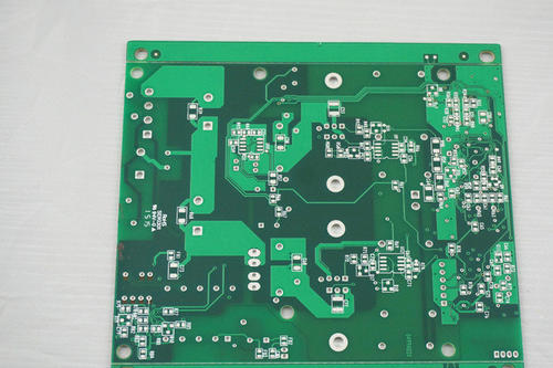
Laser processing technology is a technology that utilizes the characteristics of the interaction between laser beams and materials to cut, weld, surface treat, drill holes, micro process materials (including metals and non-metals), and use them as light sources to identify objects. The traditional application of laser processing technology is the largest field. Laser technology is a comprehensive technology that involves multiple disciplines such as optics, mechanics, electronics, materials, and detection. Traditionally, its research scope can generally be divided into: 1. Laser processing system. Including lasers, light guiding systems, machining machines, control systems, and detection systems. 2. Laser processing technology. Including various processing techniques such as cutting, welding, surface treatment, drilling, marking, marking, and fine tuning. Laser welding: Sealing devices such as thick and thin sheets of automotive body, automotive parts, lithium batteries, pacemak
Inquiry Now

