 +86 755 2794 4155
  sales@knownpcb.com
-
Shenzhen KNOWNPCB Technology Co., Ltd.
 +86 755 2794 4155
  sales@knownpcb.com
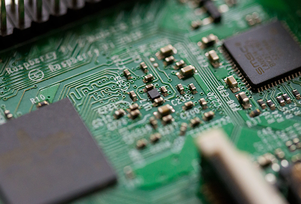
Have you noticed that now more and more of our lighting is using led lighting.What is LED? Compared to the traditional light bulbs, LEDs have lower power consumption, longer lifetime and higher energy efficiency. In the PCB industry,when we say LED PCB, it refers to the pcb used for LED lighting, if you are looking for a suitable LED PCB for your lighting system, this article may bring you something. WHAT ARE LEDS COMPOSED OF?LED is an initial light-emitting diode that produces light when an electric current passes through. LEDs typically have negative and positive electrodes, which generate light in the visible light region.The LEDS are glued to the PCB by soldering process and have electrical connections for lighting.Since light-emitting diodes dissipate a lot of heat when they are in use, when you are designing LED, the metal core is usually the best choice for LED PCB, it is because that it dissipates heat more faster. Among them, the metal material aluminum is the most widely used
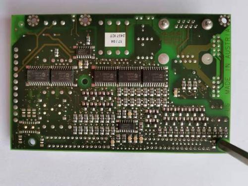
Question 1: What is part packaging and what is the difference between it and parts? Answer: (1) Part packaging refers to the appearance and solder joint position indicated when the actual part is soldered onto the circuit board. (2) Part packaging is only the appearance and solder joint position of the part, and pure part packaging is only a concept of space, so different parts can share the same part packaging; On the other hand, the same type of part can also have different packaging, such as RES2 representing resistance, which has packaging forms such as AXAIL0.4, AXAIL0.3, AXAIL0.6, etc. Therefore, when using welded parts, it is not only necessary to know the part name but also the packaging of the part. (3) The packaging of parts can be specified during circuit design or when introducing network tables. When designing a circuit diagram, you can specify it in the Footprint settings in the Part Properties dialog box, or you can also specify the part packaging when importing a
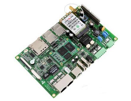
For a newly designed circuit board, debugging often encounters some difficulties, especially when the PCB board is relatively large and there are many components, making it difficult to start. But if you master a reasonable set of debugging methods, debugging will be twice the result with half the effort. For newly retrieved PCB boards, we first need to roughly observe whether there are any problems on the PCB board, such as obvious cracks, short circuits, open circuits, etc. If necessary, check if the resistance between the power supply and the ground wire is large enough. Then it's time to install the components. It is best not to install all modules that are independent of each other when you are not confident in ensuring their normal operation. Instead, you should install them part by part (for smaller circuits, you can install them all at once), which can easily determine the scope of the fault and avoid being unable to start when encountering problems. Generally speaking, th
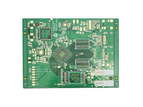
Hot air leveling is the process of immersing a printed circuit board into molten solder (63SN/37PB), and then using hot air to blow off excess solder from the surface and metalized holes of the printed circuit board, resulting in a smooth, uniform, and bright solder coating layer. The lead tin alloy coating on the surface of the printed circuit board after hot air leveling should be bright, uniform, and complete, with good solderability, no nodules or semi wetting, and the coating should be completely free of exposed copper. Copper exposure on the surface and metalized holes of the solder pad after hot air leveling is an important defect in finished product inspection, and is one of the common causes of hot air leveling rework. There are many reasons that can cause this problem, including the following. 1. Insufficient pre-treatment and poor coarsening. The quality of the pre-treatment process for PCB hot air leveling has a significant impact on the quality of hot air leveling. T
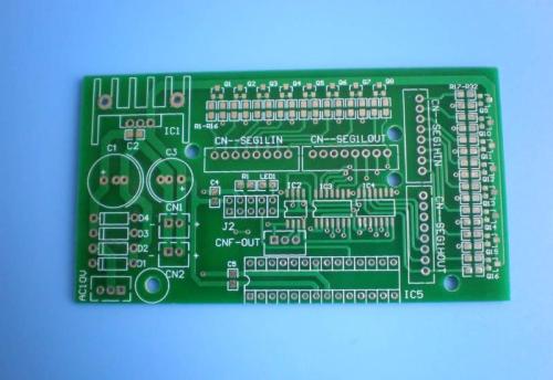
⑴ Differences in longitude and latitude directions cause changes in substrate size; Due to the lack of attention to fiber direction during shearing, shear stress remains in the substrate, and once released, it directly affects the shrinkage of the substrate size. The copper foil on the surface of the substrate is etched off, which limits the variation of the substrate and results in dimensional changes when stress is relieved. When brushing the board, excessive pressure is used, resulting in compressive and tensile stresses that cause deformation of the substrate. The resin in the substrate is not completely cured, resulting in size changes. Especially for multi-layer boards, poor storage conditions before lamination can cause moisture absorption on thin substrates or semi cured sheets, resulting in poor dimensional stability. When the multi-layer board is pressed, excessive glue flow causes deformation of the glass cloth. Solution: ⑴ Determine the variation pattern of longi
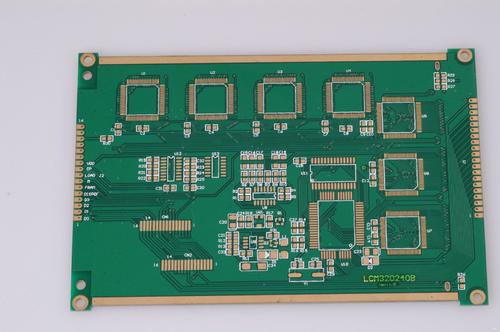
In the manufacturing process of printed circuit boards, there are many processes involved, and each process may have quality defects. These quality issues always involve many aspects, which can be difficult to solve. As the causes of problems are multifaceted, some belong to chemical, mechanical, sheet metal, optical, and other aspects. After decades of production practice, combined with practical experience in solving quality problems and relevant information on solving technical problems, the following summary is made: Defects, causes, and solutions in the manufacturing process of printed circuit boards Solution to the causes of defects in the process There are blisters on the facial mask layer of the film sticking board. The board surface is not clean. Check the wettability of the board surface, that is, the clean surface can keep the water even and the continuous water film lasts for up to 1 minute Low film temperature and pressure increase temperature and pressure The edg
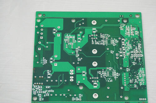
A single panel is on the most basic PCB, with parts concentrated on one side and wires concentrated on the other side. Because wires only appear on one side, we call this type of PCB a single side. Because single panels have many strict limitations in designing circuits (because they are only on one side, wiring cannot cross and must follow separate paths), only early circuits used such boards; The wiring diagram of a single panel is mainly based on screen printing, which means printing a resist on the copper surface, etching it, then marking it with solder mask, and finally completing the part guide hole and shape through punching processing. In addition, some products produced in small quantities are photographed using photosensitive agents to form patterns. Double sided boards have wiring on both sides. However, to use wires on both sides, there must be appropriate circuit connections between the two sides. The bridge between these circuits is called a guide hole (via). A guid
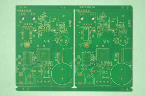
Strictly speaking, PCB double-sided board is a very important type of PCB board in the circuit board. It has a wide range of uses, and it is easy to check whether a PCB board is a double-sided board. I believe that friends can fully grasp the understanding of single panels. Double panels are the extension of single panels, which means that the circuit of single panels is not enough to turn to the opposite side. Another important feature of PCB double-sided boards is that they have conductive holes. Simply put, it means double-sided wiring, with lines on both sides! A summary is: A board with double-sided wiring is a double-sided board! Some friends may ask, for example, if a board has double-sided wiring but only one side has electronic components, is it a double-sided board or a single panel? The answer is obvious, such a board is a double-sided board, only parts are installed on the board of the double-sided board. The advantages of manufacturing PCB double-sided boards are tha
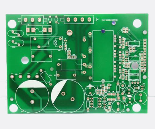
1、 Firstly, considering whether it is a customer design issue, check if there is a connection method between the solder pad and the copper sheet that may cause insufficient heating of the solder pad. 2、 Are there any issues with customer operations. If the welding method is incorrect, it will affect the insufficient heating power, temperature, and contact time. 3、 Improper storage issues. 1. Under normal circumstances, the tin sprayed surface will completely oxidize or even be shorter in about a week 2. The OSP surface treatment process can be stored for about 3 months 3. Long term preservation of sunken gold plates 4、 The issue with flux. 1. Insufficient activity to completely remove oxidation substances from PCB pads or SMD solder joints 2. Insufficient amount of solder paste at the solder joint and poor wetting performance of the flux in the solder paste 3. Part of the solder joints may not be fully filled with solder, which may result in insufficient mixing of the flux
Inquiry Now

