 +86 755 2794 4155
  sales@knownpcb.com
-
Shenzhen KNOWNPCB Technology Co., Ltd.
 +86 755 2794 4155
  sales@knownpcb.com
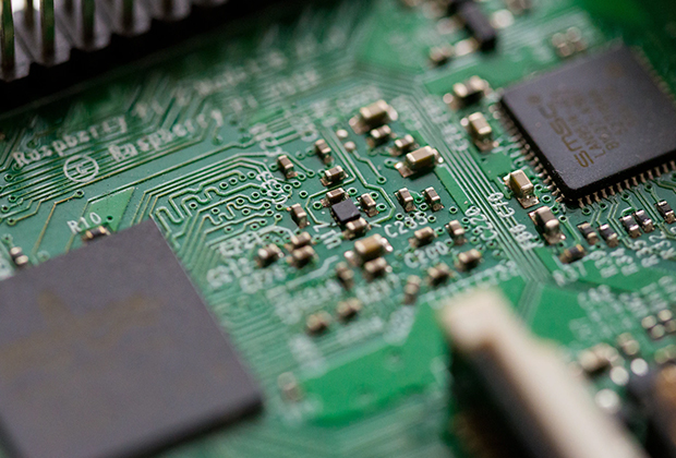
Have you noticed that now more and more of our lighting is using led lighting.What is LED? Compared to the traditional light bulbs, LEDs have lower power consumption, longer lifetime and higher energy efficiency. In the PCB industry,when we say LED PCB, it refers to the pcb used for LED lighting, if you are looking for a suitable LED PCB for your lighting system, this article may bring you something. WHAT ARE LEDS COMPOSED OF?LED is an initial light-emitting diode that produces light when an electric current passes through. LEDs typically have negative and positive electrodes, which generate light in the visible light region.The LEDS are glued to the PCB by soldering process and have electrical connections for lighting.Since light-emitting diodes dissipate a lot of heat when they are in use, when you are designing LED, the metal core is usually the best choice for LED PCB, it is because that it dissipates heat more faster. Among them, the metal material aluminum is the most widely used
Poor solderability of circuit board holes will result in virtual soldering defects, affecting the parameters of components in the circuit, leading to unstable conduction of multi-layer board components and inner wires, and causing the entire circuit function to fail. The so-called weldability refers to the property of the metal surface being wetted by molten solder, that is, the formation of a relatively uniform and continuous smooth attached film on the metal surface where the solder is located. The main factors affecting the solderability of printed circuit boards are: (1) the composition of the solder and the properties of the soldered material. Solder is an important component of the welding chemical treatment process, which is composed of chemical materials containing flux. The commonly used low melting point eutectic metals are Sn-Pb or Sn-Pb-Ag. The impurity content should be controlled in a certain proportion to prevent the oxide produced by impurities from being dissolved
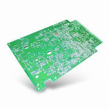
The circuit board and components undergo warping during the welding process, resulting in defects such as virtual soldering and short circuits due to stress deformation. Warping is often caused by temperature imbalance between the upper and lower parts of a circuit board. For large PCBs, the weight of the board itself can also cause warping. A regular PBGA device is about 0.5mm away from the printed circuit board. If the device on the circuit board is large, as the circuit board cools down and returns to its normal shape, the solder joints will be under stress for a long time. If the device is raised by 0.1mm, it is enough to cause a virtual solder open circuit. In terms of layout, when the circuit board size is too large, although welding is easier to control, the printed lines are longer, the impedance increases, the noise resistance decreases, and the cost increases; If it is too small, the heat dissipation will decrease, and welding will be difficult to control, making it easy
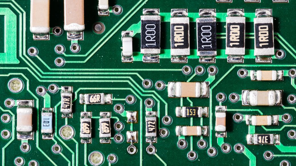
Introduce the relevant content and situation of printed circuit boards to help everyone improve their understanding. Let's read the following content together with the editor. Printed circuit boards (PCBs) are convenient thin sheets used to accommodate interconnected electrical components in a simple, convenient, and economical manner. They are used as physical supports for installing and connecting different electrical components. The PCB is made of glass fiber, composite epoxy resin or any other composite material, and has a metal coated surface. They have etching made of metals and acids to create circuits through different integrated circuits (ICs) and other components on circuit boards. Solder connects ICs and other components to the surface of the circuit board. The copper tracks in the circuit board reduce the possibility of short circuits, misalignment, or misaligned wires. In this way, all components are firmly fixed to the circuit board without the need for complex wirin
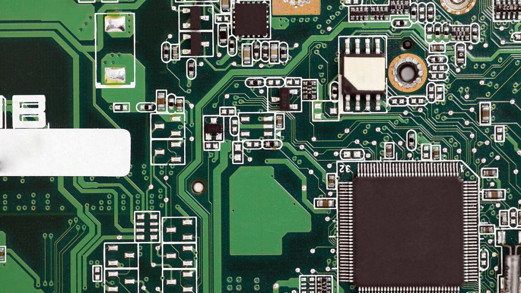
The so-called copper coating refers to using the idle space on the PCB as a reference plane, and then filling it with solid copper. These copper areas are also known as copper filling. Copper coating can be divided into large-area copper coating and grid copper coating. Next, let professional PCB manufacturers provide you with a detailed understanding of the basic knowledge of PCB circuit board copper coating: 1、 Precautions for copper coating: 1. Single point connection in different locations: connected through a 0 ohm resistor, magnetic bead, or inductor. 2. The copper coating near the crystal oscillator is used as a high-frequency emission source in the circuit. The crystal oscillator should be surrounded by copper coating, and then the outer shell of the crystal oscillator should be grounded separately. 2、 What are the benefits of copper coating? 1. Copper coating can reduce ground wire impedance and improve anti-interference ability; 2. Reduce voltage drop and improve po
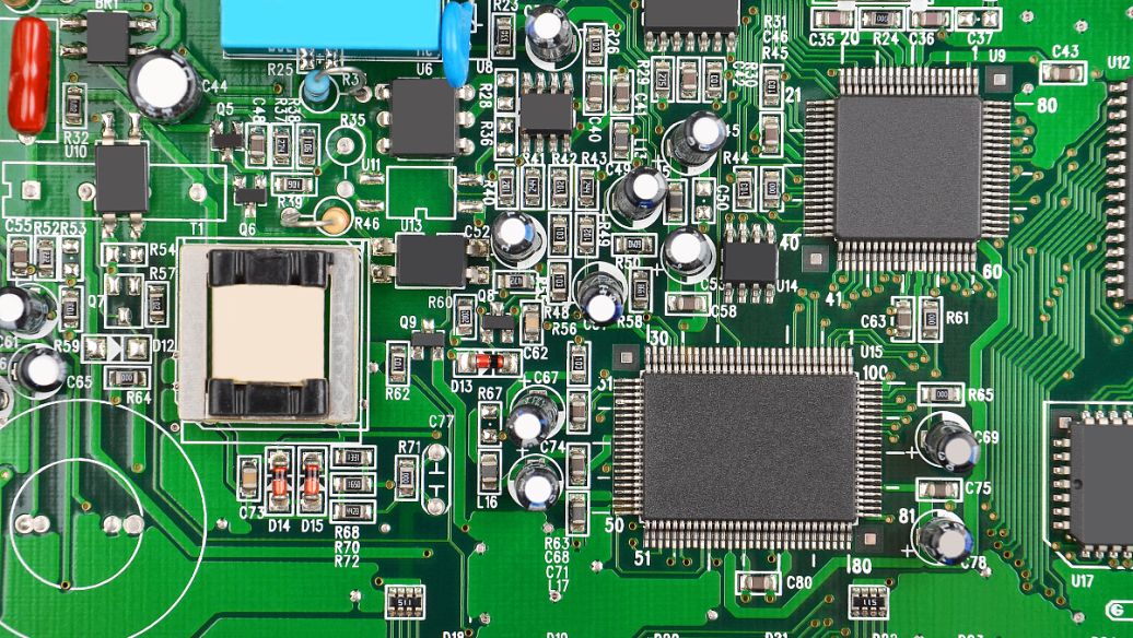
In the field of PCB, there are often many English terms that industry insiders may find difficult to fully recognize. How much do you know about PCB terminology? Let me introduce some commonly used terms in the PCB field to you: 1. FR4 In most cases, the glass fiber substrate for PCBs generally refers to the material "FR4". The solid material "FR4" gives PCB hardness and thickness. Some cheap PCBs are made of materials such as epoxy resin or phenol, lacking the durability of FR4, but they are much cheaper. Phenolic substances have a lower thermal decomposition temperature, and excessive welding time can lead to their decomposition and carbonization, and emit unpleasant odors. 2. Copper The thin copper foil layer on a PCB is pressed onto the substrate through heat and adhesive during production. On double-sided boards, copper foil is pressed onto both sides of the substrate. When we mention "double-sided board" or "two-layer board", we refer to two layers of copper foil on a th
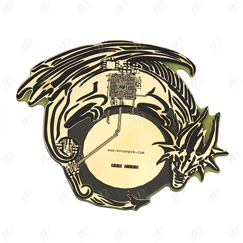
On PCBs, nickel is used as a substrate coating for precious and base metals. The deposition layer of low stress nickel on PCB is usually prepared using modified Watt nickel plating solution and some amino sulfonic acid nickel plating solution with stress reducing additives. What are the common problems encountered when using PCB nickel plating solution, as analyzed by CITIC Huawei? 1、 Temperature - Different nickel processes use different plating bath temperatures. In nickel plating solutions with higher temperatures, the obtained nickel coating has low internal stress and good ductility. The general operating temperature is maintained at 55-60 degrees Celsius. If the temperature is too high, nickel salt hydrolysis will occur, causing pinholes in the coating and reducing cathodic polarization. 2、 PH value - The pH value of nickel plating electrolyte has a significant impact on the performance of the coating and electrolyte. The pH value of PCB nickel plating electrolyte is genera
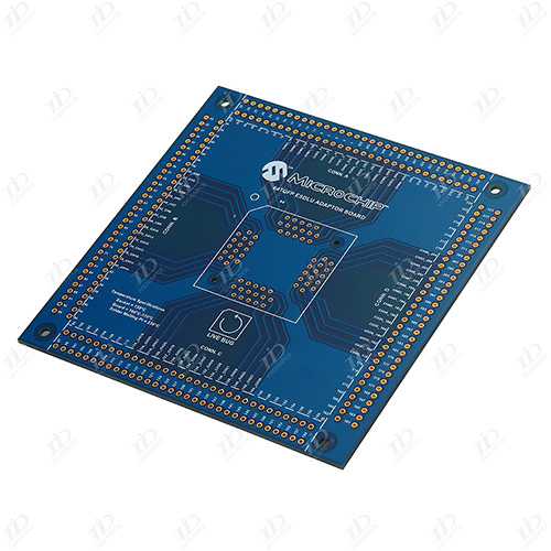
In PCB sampling, nickel is used as a substrate coating for precious and base metals. For some surfaces with heavy load wear, using nickel as the gold substrate coating can greatly improve wear resistance. When used as a barrier layer, nickel can effectively prevent the diffusion between copper and other metals. Next, CITIC Huawei will explain the causes and solutions of PCB nickel plating process faults: 1、 Ma Keng: Ma Keng is the result of organic pollution; If the stirring is poor, bubbles cannot be expelled and pits will form. Large pits usually indicate oil contamination, and wetting agents can be used to reduce their impact. Small pits are called pinholes, which can be caused by poor treatment, metal impurities, low boric acid content, and low plating temperature. Bath maintenance and process control are key, and anti pinhole agents should be used as process stabilizers to supplement. 2、 Roughness and burrs: Roughness indicates that the solution is dirty, which can be correc
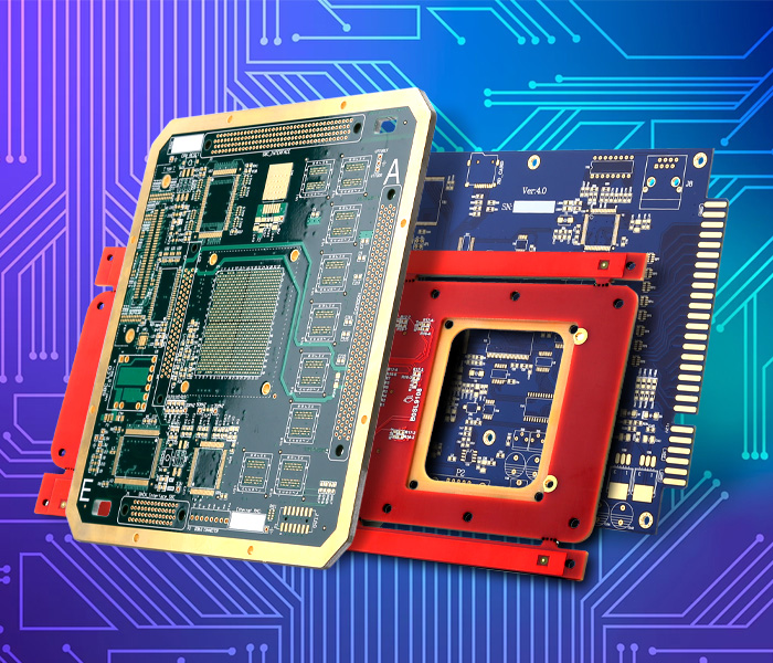
The volume of electronic products is becoming increasingly thin and short, and directly stacking holes on through blind holes is a design method to achieve high-density interconnection. To achieve good hole stacking, the first step is to ensure the flatness of the hole bottom. There are several typical methods for making flat hole surfaces, and electroplating hole filling process is one of the representative ones. The electroplating hole filling process can not only reduce the necessity of additional process development, but also be compatible with current process equipment, which is conducive to achieving good reliability. So, what factors affect the PCB electroplating hole filling process? In PCB sampling, the influence of substrate on electroplating hole filling cannot be ignored, generally including factors such as dielectric layer material, hole shape, thickness to diameter ratio, and chemical copper coating. (1) Medium layer material. The material of the dielectric layer ha
Inquiry Now

