 +86 755 2794 4155
  sales@knownpcb.com
-
Shenzhen KNOWNPCB Technology Co., Ltd.
 +86 755 2794 4155
  sales@knownpcb.com
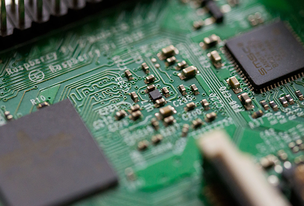
Have you noticed that now more and more of our lighting is using led lighting.What is LED? Compared to the traditional light bulbs, LEDs have lower power consumption, longer lifetime and higher energy efficiency. In the PCB industry,when we say LED PCB, it refers to the pcb used for LED lighting, if you are looking for a suitable LED PCB for your lighting system, this article may bring you something. WHAT ARE LEDS COMPOSED OF?LED is an initial light-emitting diode that produces light when an electric current passes through. LEDs typically have negative and positive electrodes, which generate light in the visible light region.The LEDS are glued to the PCB by soldering process and have electrical connections for lighting.Since light-emitting diodes dissipate a lot of heat when they are in use, when you are designing LED, the metal core is usually the best choice for LED PCB, it is because that it dissipates heat more faster. Among them, the metal material aluminum is the most widely used
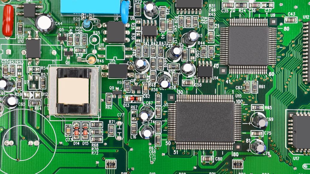
1. Crystal foil phenolic glass layer pressure plate: It is a layer of pressure products made of epoxy phenolic resin through the heat pressure of epoxy phenol. Good performance and convenient processing. Its plate surface is pale yellow. If the triamine is used as a curing agent, the surface of the plate is pale green and has good transparency. It is mainly used as printed circuit boards in radio equipment with high working temperature and frequency. 2. Copper foil phenolic paper layer pressure plate: It is a layer pressure product made of phenolic resin perfume with phenolic resin through the heat pressure of phenolic resin. Comes with a single -alkali glass soaked tape, and it is applied to copper foil. It is mainly used as a printed circuit board in radio equipment. 3. Soft polyester copper film: It is a band -shaped material made of polyester film and copper thermal, and it curls into spiral shape inside the device in the application. In order to reinforce or moisture -proof,
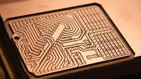
1. Layout The layout, line width, and line spacing of printed wires and pads shall be in accordance with the provisions of the design drawings. But our company will handle the following: compensate for the line width and PAD ring width appropriately according to the process requirements, and generally increase the PAD for single panels as much as possible to enhance the reliability of customer welding. When the design line spacing does not meet the process requirements (if it is too dense, it may affect performance and manufacturability), our company will make appropriate adjustments according to the pre production design specifications. ★ In principle, it is recommended that customers design double or multi-layer boards with a through hole (VIA) inner diameter of 0.3mm or more and an outer diameter of 0.6mm or more. The component pad should be greater than 50% of the aperture, and the minimum plate thickness to aperture ratio should be ≤ 6:1. The design of the width and spacing o
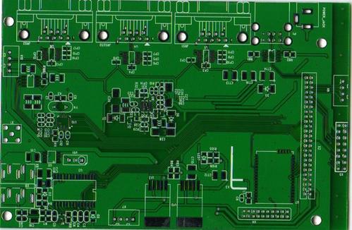
1. The various design elements that make up a PCB should be described in the design drawings. The appearance is represented by Mechanical 1-16 layers (priority) or Keep out layer. If used simultaneously in the design file, generally keep out layer is used to prohibit wiring without opening holes, and mechanical 1 is used to indicate forming. In the design pattern, indicate a long SLOT hole or hollow, and use Mechanical 1 layer to draw the corresponding shape. 2. Dimensional tolerances for PCB board samples The overall dimensions of the PCB should comply with the provisions of the design drawings. When there is no specification in the drawing, the tolerance of the external dimensions is ± 0.2mm. 3. Flatness (warpage) 0.7% (4) The concept of layers 1. If a single panel draws a signal layer on the top layer, it indicates that the circuit on that layer is the front view. 2. If a single panel draws a signal layer on the bottom layer, it indicates that the circuit on that layer is
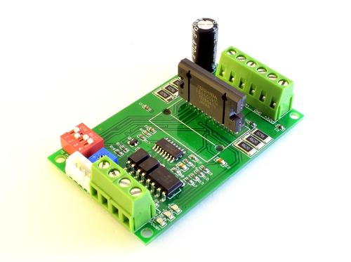
PCB (Printed Circuit Board), also known as Printed Circuit Board or Printed Circuit Board in Chinese, is an important electronic component that supports electronic components and provides electrical connections for electronic components. Due to its use of electronic printing technology, it is called a "printed" circuit board. The early 20th century to the late 1940s was the embryonic stage of the development of PCB substrate materials industry. Its development characteristics are mainly reflected in the emergence of a large number of resin, reinforcement materials, and insulation substrates used by professional PCB manufacturers for substrate materials during this period, and preliminary technological exploration has been made. All of these have created necessary conditions for the emergence and development of the most typical substrate material for printed circuit boards - copper-clad board. On the other hand, the mainstream PCB manufacturing technology, which uses metal foil etc
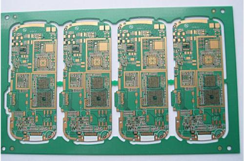
PCB (Printed Circuit Board), also known as Printed Circuit Board or Printed Circuit Board in Chinese, is an important electronic component that supports electronic components and provides electrical connections for electronic components. Due to its use of electronic printing technology, it is called a "printed" circuit board. The early 20th century to the late 1940s was the embryonic stage of the development of PCB substrate materials industry. Its development characteristics are mainly reflected in the emergence of a large number of resin, reinforcement materials, and insulation substrates used by professional PCB manufacturers for substrate materials during this period, and preliminary technological exploration has been made. All of these have created necessary conditions for the emergence and development of the most typical substrate material for printed circuit boards - copper-clad board. On the other hand, the mainstream PCB manufacturing technology, which uses metal foil etc
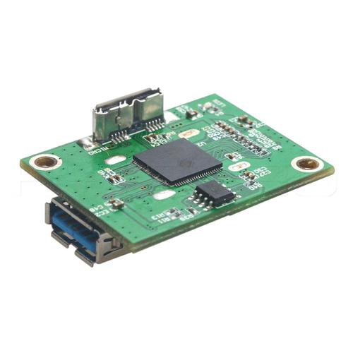
1. The multi-layer PCB board has good sampling quality and strong wear resistance. The surface of the PCB board sample is clearly and aesthetically pleasing, and can be marked with various logos, patterns, QR codes, and text. The patterns are directly engraved on the material, which highlights the wear resistance; 2. High machining accuracy. The minimum spot diameter of the laser beam emitted by the laser can reach 10um (UV laser) after being focused, which is of great help in processing complex graphics and precision machining; 3. High efficiency, simple operation, and cost reduction. Users only need to set the parameters on the computer to directly mark the material surface, which can be completed in just a few seconds to more than ten seconds; 4. Non destructive marking. Laser marking adopts non-contact processing, and the laser head does not need to contact the surface of the material, so there is no need to consider damage to the material; 5. Wide range of use, safe and en
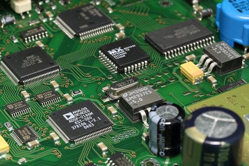
1. Substrate ★ FR4: Glass cloth epoxy resin copper-clad foil plate (Tg: 130 °). ★ CEM-1: Paper core glass cloth surface - epoxy resin copper-clad foil board. ★ 94V0: Flame retardant cardboard. ★ Aluminum substrate: Thermal conductivity coefficient of 100. 2. Copper foil: 99.9% or more electrolytic copper, surface copper foil thickness of finished product: 18 μ M (H/HOZ), 35 μ M (1OZ), 70 μ M (2OZ). 3. Plate thickness: ★ Thickness of single and double-sided boards: 0.4mm, 0.6mm, 0.8mm, 1.0mm, 1.2mm, 1.6mm, 2.0mm, 2.5mm The minimum thickness of multi-layer printed boards: 4 layers ≥ 0.6mm, 6 layers ≥ 1.0mm, and 8 layers ≥ 1.6mm, with a finished board thickness tolerance of ± 10%.
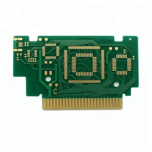
1. The less bending the leads between the pins of high-speed electronic devices, the better. It is best to use full straight leads for high-frequency circuit wiring, and if a bend is needed, a 45 degree bend or arc bend can be used. This requirement is only used to improve the bonding strength of copper foil in low-frequency circuits, while in high-frequency circuits, meeting this requirement can reduce the external emission and mutual coupling of high-frequency signals. 2. The less interlayer alternation between the pins of high-frequency circuit devices, the better. The so-called "less interlayer alternation of the leads, the better" refers to the use of fewer via (Via) during the component connection process. A through-hole can bring about a distributed capacitance of about 0.5pF, reducing the number of through-holes can significantly improve speed and reduce the possibility of data errors. 3. The shorter the lead between the pins of high-frequency circuit devices, the better.
Inquiry Now

