 +86 755 2794 4155
  sales@knownpcb.com
-
Shenzhen KNOWNPCB Technology Co., Ltd.
 +86 755 2794 4155
  sales@knownpcb.com
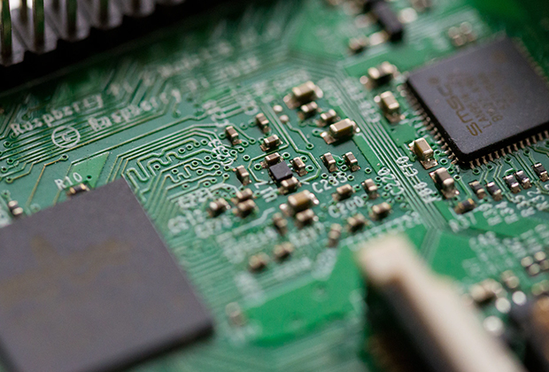
Have you noticed that now more and more of our lighting is using led lighting.What is LED? Compared to the traditional light bulbs, LEDs have lower power consumption, longer lifetime and higher energy efficiency. In the PCB industry,when we say LED PCB, it refers to the pcb used for LED lighting, if you are looking for a suitable LED PCB for your lighting system, this article may bring you something. WHAT ARE LEDS COMPOSED OF?LED is an initial light-emitting diode that produces light when an electric current passes through. LEDs typically have negative and positive electrodes, which generate light in the visible light region.The LEDS are glued to the PCB by soldering process and have electrical connections for lighting.Since light-emitting diodes dissipate a lot of heat when they are in use, when you are designing LED, the metal core is usually the best choice for LED PCB, it is because that it dissipates heat more faster. Among them, the metal material aluminum is the most widely used
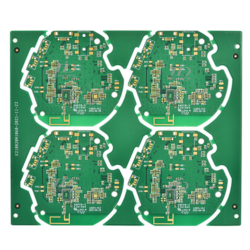
The through hole plays a role in connecting and conducting circuits, and the development of the electronics industry has promoted the development of PCBs, resulting in the emergence of plug hole technology. In order to meet the customer's requirements, the process of conducting and plugging holes can be described as diverse, with a particularly long process flow and difficult process control. So, how is the process of plugging through holes in PCB circuit boards achieved? Let's take a look together with the editor: 1、 Plug hole process after hot air leveling This process flow is: board surface resistance welding → HAL → plug hole → curing. Production is carried out using a non plug hole process, and after hot air leveling, aluminum mesh plates or ink blocking nets are used to complete the plug holes of all fortresses. Plug ink can be used as photosensitive ink or thermosetting ink. This process flow can ensure that the guide hole does not fall off oil after hot air leveling, but
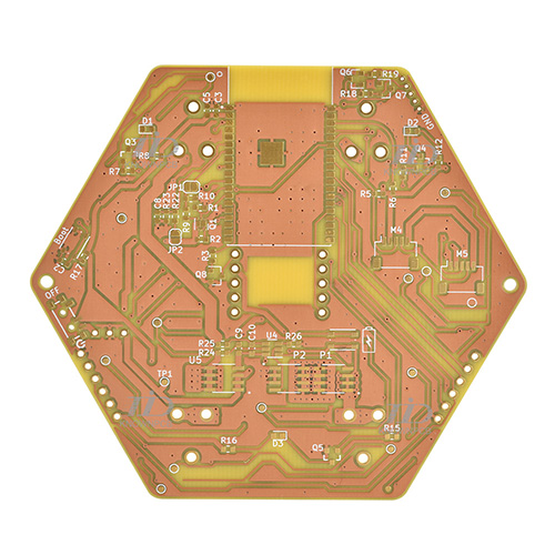
(1) There should be a reasonable direction: such as input/output, AC/DC, strong/weak signals, high-frequency/low-frequency, high-voltage/low-voltage, etc. Their direction should be linear (or separated) and should not blend with each other. Its purpose is to prevent mutual interference. (2) Choose a good grounding point: For example, the multiple ground wires of the forward amplifier should be merged before connecting to the main ground, etc. (3) Reasonably arrange the power filter/decoupling capacitors: Generally, only a few power filter/decoupling capacitors are drawn in the schematic diagram, but they are not indicated where they should be connected. In fact, these capacitors are designed for switching devices or other components that require filtering/decoupling, and they should be arranged as close to these components as possible. (4) There is a particular emphasis on lines: if conditions permit, lines that are wide will never be thin; High voltage and high-frequency lines
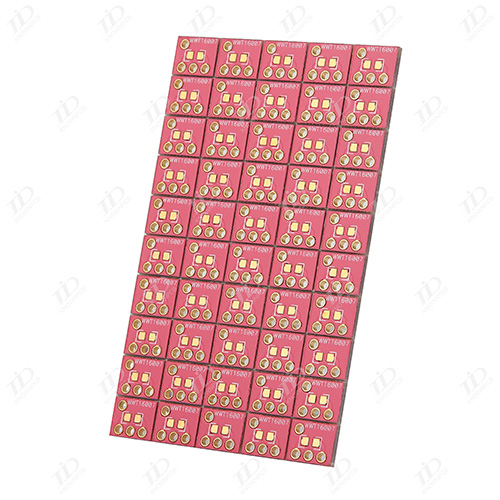
What are the design requirements for PCB printed circuit boards in PCB sampling? Let's take a look together: 1. Accurate This is the most basic and important requirement for printed circuit board design. Accurately implement the connection relationship of the electrical schematic diagram to avoid errors such as "short circuit" and "open circuit". Generally, products need to undergo more than two rounds of trial production and modification, while CAD software with strong functions has inspection functions to ensure the correctness of electrical connections. 2. Reliable A correctly connected circuit board may not necessarily have good reliability, such as improper selection of boards, incorrect board thickness and installation fixation, improper component layout and wiring, etc., which may cause the PCB to not work reliably. 3. Reasonable A printed circuit board component is closely related to the rationality of the printed circuit board, from manufacturing, inspection, assembl

The circuit board sampling of circuit board manufacturers generally refers to the electronic products being sent to the circuit board manufacturer for processing into circuit boards for testing after the engineer completes the PCB layout design. Because it is a newly developed product, many functions are not yet perfect, and there are still many functions that need to be debugged. Only after debugging is qualified can batch production be carried out. If debugging is not qualified, it is necessary to revise, sample, and debug again, reducing a lot of unnecessary hemp in the later stage The quantity of samples varies depending on the delivery time of the samples. Generally speaking, for an ordinary single and double-sided board, it is not urgent, with a quantity of less than 10 pieces and a standard process. The scale is within 100 * 100mm, and it usually costs only 50 yuan. However, if your quantity is larger than this, and the delivery time needs to be expedited, the price will va
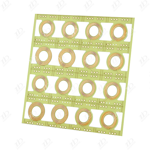
Generally, a well made PCB board diagram needs to be processed and manufactured by the board manufacturer. After the sample is completed, technicians will weld the components together, and finally assemble them into the shell and package them to form a complete product. So what relevant document parameters and explanations are required for PCB sampling to be provided to the manufacturer? Let me explain them in detail below. What are the relevant document parameters and explanations provided to the manufacturer for PCB sampling requirements 1. PCB sampling data: To clarify what kind of manufacturing data is required for PCB, the most common method currently is to use FR4, and the primary data is epoxy resin peeled fiber cloth board. 2. Layer: To clarify the number of layers you manufacture for PCB boards. (The manufacturing layers of PCB boards vary, and the price may vary, while the sampling process for PCB circuit boards is completely different.) 3. Solder resistance color: The
1. The thickness of gold is much thicker than that of gold plating, and sinking gold will produce a golden yellow color that is more yellow than plating, which is more satisfying for customers. 2. Compared to gold plating, sinking gold is easier to weld and will not cause welding defects, leading to customer complaints. The stress on the sinking gold plate is easier to control, which is more conducive to the processing of products with bonding. It is precisely because sinking gold is softer than plating gold that sinking gold plates make gold fingers less wear-resistant. 3. As long as there is nickel gold on the solder pad of the sinking gold plate, the signal transmission in the skin effect will not be affected by the copper layer. 4. Compared to gold plating, sinking gold has a denser crystal structure and is less prone to oxidation. 5. As the wiring becomes denser, the line width and spacing have now reached 3-4 MIL. Gold plating is prone to short circuits in the gold wire.
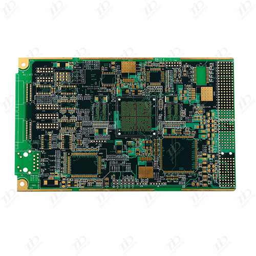
1、 Quality requirements and key control points for PCB etching process: 1. There should be no residual copper in the sample production of PCB boards, especially double-sided boards, which should be noted. 2. There must be no residual adhesive present, otherwise it will result in exposed copper or poor adhesion of the coating. 3. The etching speed should be appropriate, and it is not allowed to show the thinning of the line caused by excessive etching. The etching line width and total pitch should be the focus of our station's control. 4. The dry film on the solder joints of the circuit shall not be washed away or cracked. 5. After etching and peeling, the board should not have any oil stains, impurities, copper skin warping or other poor quality. 6. When placing the board, attention should be paid to preventing jamming and oxidation. 7. It should be ensured that the etching solution is evenly distributed to prevent uneven etching of different parts on the front and back or t
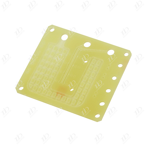
With the continuous development of the electronics industry, various electronic products are emerging one after another. Often, some customers demand unconventional thickness boards, such as 2.0mm, 2.4mm, 2.5mm, 3.0mm thick, etc. Can 3.0mm thickness boards be produced? The answer is revealed below, and the editor will explain it in detail below. In order to ensure the integrity of product functionality, many customers choose thicker boards for production when their boards are used on equipment or when the components on the boards are heavy. The normal board thicknesses we produce are 0.6mm, 0.8mm, 1.0mm, 1.2mm, and 1.6mm. Some special products require thicker PCB boards. Use thicker PCB boards. Can we ultimately make a 3.0mm thick PCB sample. The answer is certain, it can be produced. Our company often produces this type of board, and producing PCBs of this thickness is no longer a challenge in the industry. Only engineers need to pay attention when planning. When planning, it i
Inquiry Now

