 +86 755 2794 4155
  sales@knownpcb.com
-
Shenzhen KNOWNPCB Technology Co., Ltd.
 +86 755 2794 4155
  sales@knownpcb.com
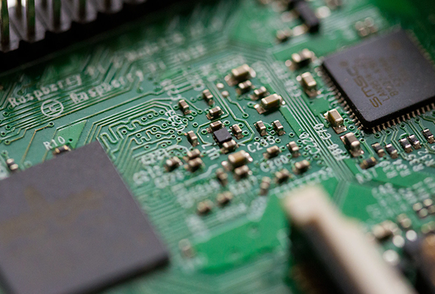
Have you noticed that now more and more of our lighting is using led lighting.What is LED? Compared to the traditional light bulbs, LEDs have lower power consumption, longer lifetime and higher energy efficiency. In the PCB industry,when we say LED PCB, it refers to the pcb used for LED lighting, if you are looking for a suitable LED PCB for your lighting system, this article may bring you something. WHAT ARE LEDS COMPOSED OF?LED is an initial light-emitting diode that produces light when an electric current passes through. LEDs typically have negative and positive electrodes, which generate light in the visible light region.The LEDS are glued to the PCB by soldering process and have electrical connections for lighting.Since light-emitting diodes dissipate a lot of heat when they are in use, when you are designing LED, the metal core is usually the best choice for LED PCB, it is because that it dissipates heat more faster. Among them, the metal material aluminum is the most widely used
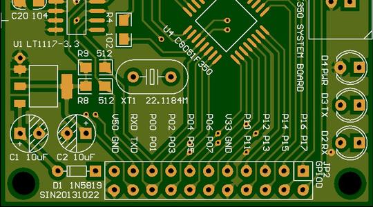
When copper plating, the low current area of the circuit board surface appears "dull" phenomenon, and the chlorine concentration is low; Generally, after adding hydrochloric acid, the "dull" phenomenon of the coating in the low current density area of the plate can disappear, the chloride ion concentration in the plating solution can reach the normal range, and the plate coating is bright. If a large amount of hydrochloric acid is added to solve the "dull" phenomenon of the coating in the low current density area, it is not necessarily caused by too low chloride ion concentration, and the real reason needs to be analyzed. If you take to add a large amount of hydrochloric acid: one, may have other consequences, two to increase production costs, is not conducive to enterprise competition. Correct analysis of "low current density area coating luster" reasons: By adding a large amount of hydrochloric acid to eliminate the "low current density area coating is not bright" phenomenon, i
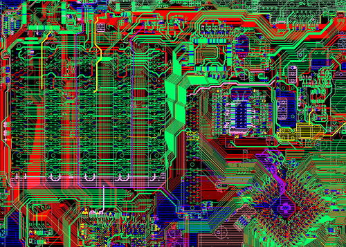
Vacuum laminating machine, reduce the pressure to reduce the flow of glue, try to maintain more resin amount, because the resin affects εr, resin preservation more, εr will be lower. Control laminate thickness tolerances. Because the thickness of the PCB board is not uniform, it indicates that the change in the thickness of the medium will affect Z0. Strictly according to the customer requirements of the PCB board plate type, the model is wrong, εr is wrong, the board thickness is wrong, the manufacturing process of PCB is all right, and the same is scrapped. Because Z0 is greatly affected by εr, the finished multilayer board should try to avoid water absorption, because the εr of water = 75, which will bring a great drop and instability effect on Z0. The solder resistance of the PCB board surface will reduce the Z0 value of the signal line by 1 to 3Ω, and theoretically the solder resistance thickness should not be too thick, in fact, the impact is not very large. The surface of
The design of dynamic circuits is aimed at the repeated bending that occurs throughout the entire lifecycle of a product, such as cables for printed machines and disk drives. In order to achieve the longest bending life cycle of the dynamic circuit, the relevant parts should be designed as a single-sided circuit with copper on the central axis. The central axis refers to a theoretical plane located at the central layer of the material that makes up the circuit. By using the same thickness of substrate film and lamination on both sides of copper, the copper foil will be accurately positioned in the center and subjected to minimal pressure during bending or bending. The design of multi-layer complexity that requires high dynamic bending cycles and high density can now be achieved by using anisotropic (z-axis) adhesives to connect double-sided or multi-layer circuits to single-sided circuits. Bending only occurs in the area of single-sided assembly, and outside the dynamic bending ar

There are two different structures for circuit boards: core structure and foil structure. In the core structure, all conductive layers in the circuit board are laid on the core material; In the foil structure, only the internal conductive layer of the circuit board is applied to the core material, and the external conductive layer is made of a foil dielectric plate. All conductive layers are bonded together through a multi-layer lamination process using a medium. Nuclear materials are double-sided foil plates used in factories. Because each core has two faces, when fully utilized, the number of conductive layers on the PCB is even. Why not use foil on one side and nuclear structure on the other? The main reason is the cost of PCB and the curvature of PCB.
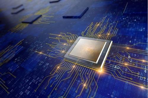
PCB (Printed Circuit Board), the Chinese name is a printed circuit board, also known as the printing circuit board, is an important electronic component, a supporting body for electronic components, and a carrier for electronic components. Because it is made of electronic printing, it is called a "print" circuit board. Act After the electronic equipment uses the printed board, due to the consistency of similar printed boards, it avoids the errors of artificial wiring, and can realize the automatic installation or paste, automatic welding, and automatic detection of electronic components, which ensures the quality of electronic equipment , Increase labor productivity, reduce costs, and facilitate maintenance. Classification (1) Single panel Single-Sided Boards is on the most basic PCB, parts of the parts on one side, and the wires are concentrated on the other side (when there is a patch component, the wire is the same side, and the plug-in device is another). (2) Double -panel
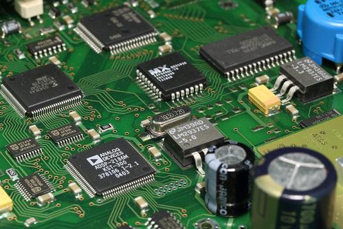
Due to the lack of one layer of dielectric and foil, the cost of raw materials for odd numbered PCBs is slightly lower than that for even numbered PCBs. However, the processing cost of odd layer PCBs is significantly higher than that of even layer PCBs. The processing cost of the inner layer is the same; But the foil/core structure significantly increases the processing cost of the outer layer. Odd layer PCBs require the addition of non-standard stacked core bonding processes on the basis of core structure technology. Compared to the nuclear structure, the production efficiency of factories that add foil outside the nuclear structure will decrease. Before laminating and bonding, the outer core requires additional processing, which increases the risk of scratches and etching errors on the outer layer. The best reason for not designing PCBs with odd layers is that odd layer circuit boards are prone to bending. When the PCB is cooled after the multi-layer circuit bonding process, th
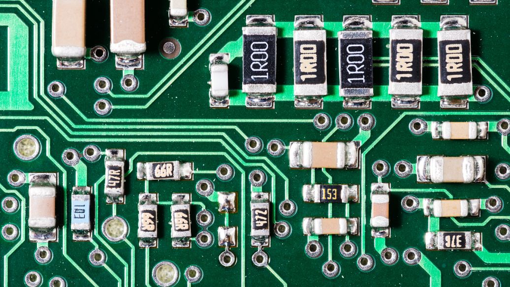
The current boards are rarely that kind of rectangular or other. They are all irregular, but there are several kinds of line drawing outer frames, which are unable to choose from. In addition, now because of the use of the equipment (such as SMT), now They all have to spell V-CUT, but the spacing spacing is different, some have spacing, and some have no distance. It is okay to do a batch for the first factory. It is not possible to fight according to the first factory, and the steel net cannot be set. Therefore, there is no special case, it is best not to have a spacing; in addition, some file design may draw a small cubic hole to draw a small cubic hole on the shape layer. Compared to PADS, it is better to put it on the appearance layer. It is easy to misunderstand the manufacturer as to rush out this hole or make the NPTH attribute. For some PTH attributes, it is easy to have problems.
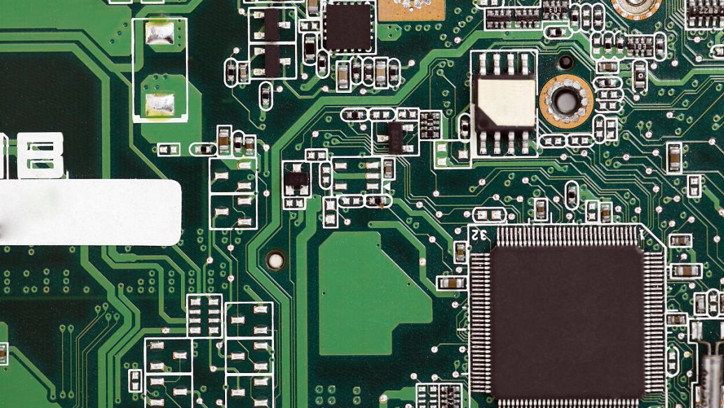
PCB heat dissipation. For electronic devices, a certain amount of heat will generate during work, so that the internal temperature of the equipment will rise rapidly. If the heat is not distributed in time, the equipment will continue to heat up, and the device will fail due to overheating. Electronics will fail. Electronics will fail. Electronics will fail. Electronics will be invalidated. The reliability of the device will decrease. Therefore, it is very important to carry out a good heat dissipation treatment on the circuit board. The heat dissipation of the PCB circuit board is a very important link, so what are the cooling skills of the PCB circuit board? Let's discuss it together. 1. PCB plates that are widely used through the PCB board itself are copper -covered/epoxy glass cloth substrates or phenolic resin glass cloth substrates, as well as a small amount of paper base covering copper plate. Although these substrates have excellent electrical performance and processing p
Inquiry Now

