 +86 755 2794 4155
  sales@knownpcb.com
-
Shenzhen KNOWNPCB Technology Co., Ltd.
 +86 755 2794 4155
  sales@knownpcb.com
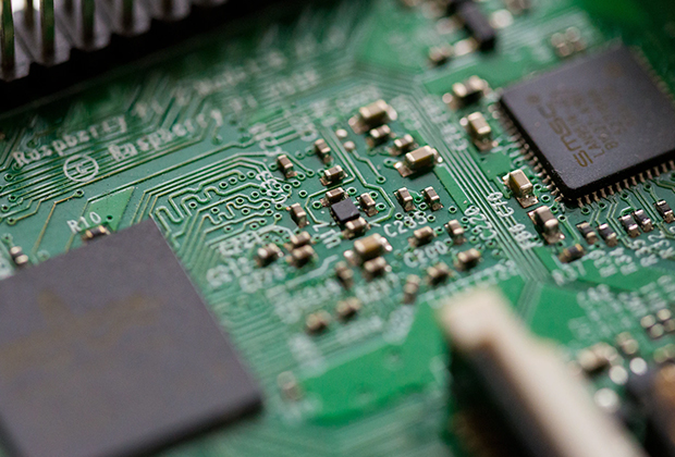
Have you noticed that now more and more of our lighting is using led lighting.What is LED? Compared to the traditional light bulbs, LEDs have lower power consumption, longer lifetime and higher energy efficiency. In the PCB industry,when we say LED PCB, it refers to the pcb used for LED lighting, if you are looking for a suitable LED PCB for your lighting system, this article may bring you something. WHAT ARE LEDS COMPOSED OF?LED is an initial light-emitting diode that produces light when an electric current passes through. LEDs typically have negative and positive electrodes, which generate light in the visible light region.The LEDS are glued to the PCB by soldering process and have electrical connections for lighting.Since light-emitting diodes dissipate a lot of heat when they are in use, when you are designing LED, the metal core is usually the best choice for LED PCB, it is because that it dissipates heat more faster. Among them, the metal material aluminum is the most widely used

It has been said that there are only two types of electronics engineers in the world: those who have experienced electromagnetic interference and those who have not. With the increase of PCB routing, electromagnetic compatibility design is an issue that we electronic engineers have to consider. Faced with a design, there are five important attributes to consider when conducting an EMC analysis of a product and design: (1) Key device size: the physical size of the emitting device that produces radiation. The radio frequency (RF) current will generate an electromagnetic field, which will leak out of the housing through the housing. The line length on the PCB as a transmission path has a direct impact on the RF current. (2) Impedance matching: the impedance of the source and receiver, and the transmission impedance between the two. (3) The temporal nature of the interference signal: whether the problem is a continuous (periodic signal) event, or only exists in a specific operating
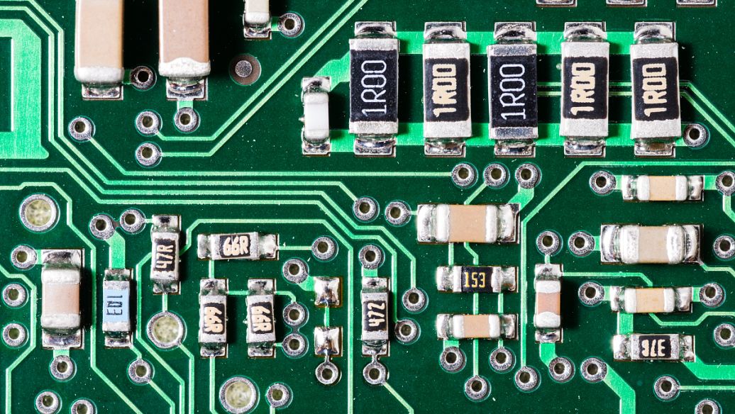
1, it is mentioned above that ordinary electrolytic copper foil is galvanized or copper-plated products, if the peak value of the wool foil production is abnormal, or galvanized/copper plating, the coating crystal branch is bad, resulting in the peel strength of the copper foil itself is not enough, the bad foil pressing board is made of PCB plug-in in the electronics factory, the copper wire will fall off by external impact. This kind of bad copper stripping copper wire to see the copper foil surface (that is, the contact surface with the substrate) will not be obvious side corrosion, but the peeling strength of the whole copper foil will be very poor. 2, poor adaptability of copper foil and resin: some special properties of laminates now used, such as HTg sheet, because the resin system is not the same, the curing agent used is generally PN resin, resin molecular chain structure is simple, the degree of cross-linking is low when curing, is bound to use special peak copper foil and
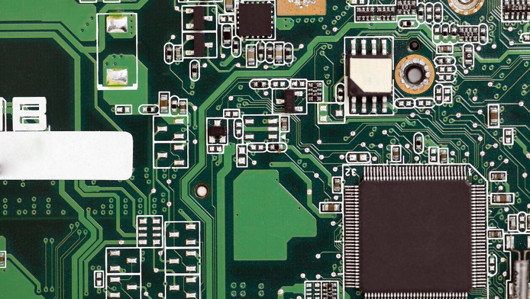
PCB printed circuit board drilling, the use of the upper and lower plate is to prevent the surface of the board and the bottom surface of the copper foil to produce burrs, so that the surface of the board drilling smooth improve the quality of the PCB printed circuit board, improve the yield. Due to the use of this auxiliary material has a certain cost, but due to the above reasons, it is in fact necessary to use, which can greatly improve the pass rate of the product and reduce the cost. The requirements for the board drilling are: there is a certain surface hardness to prevent burrs on the surface of the drilling. But not too hard to wear the drill. It is required that the resin composition of the upper and lower backing plate should not be too high, otherwise a molten resin ball will be formed when drilling and adhere to the hole wall. The larger the thermal conductivity, the better, so that the heat generated during drilling can be quickly taken away, reduce the temperature of
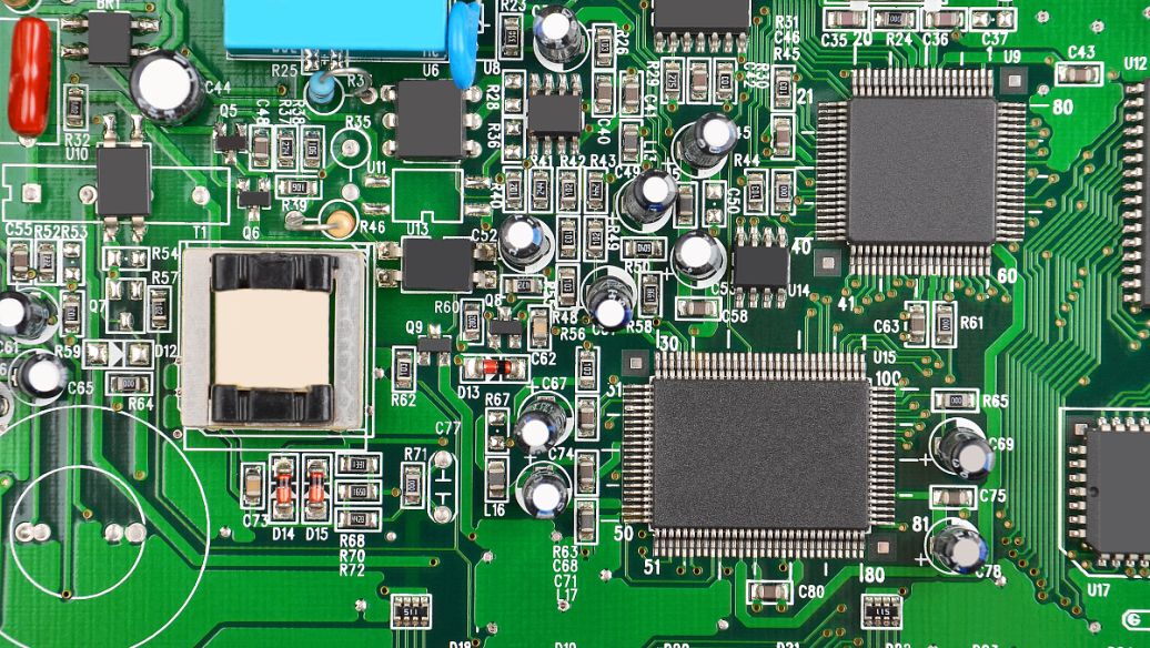
1, copper foil etching is excessive, the electrolytic copper foil used on the market is generally single-sided galvanized (commonly known as ashing foil) and single-sided plated copper (commonly known as reddened foil), the common copper is generally more than 70um galvanized copper foil, reddening foil and 18um below the ashing foil basically have not appeared batch copper. When the customer line design is better than the etching line, if the copper foil specifications are changed and the etching parameters are not changed, the residence time of the copper foil in the etching solution is too long. Because zinc is originally a active metal, when the copper wire on the PCB is soaked in the etching liquid for a long time, it will lead to excessive side corrosion of the line, causing some fine line backing zinc layer to be completely reacted off and separated from the substrate, that is, the copper wire falls off. There is also a case that there is no problem with PCB etching paramete
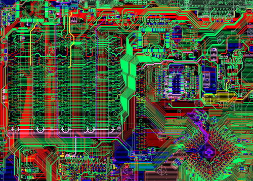
First, it is used as an electrical connection between the layers; The second is used as the fixing or positioning of the device. If you look at the process, these holes are generally divided into three categories, namely blind via, buried via and through via. Blind holes are located on the top and bottom surfaces of the printed circuit board and have a certain depth for the connection of the surface circuit and the inner circuit below, and the depth of the holes usually does not exceed a certain ratio (aperture). The buried hole refers to the connection hole located in the inner layer of the printed circuit board, which does not extend to the surface of the board. The above two types of holes are located in the inner layer of the circuit board, which is completed by the through hole molding process before lamination, and several inner layers may be overlapped during the formation of the through hole. The third type is called through-holes, which pass through the entire circuit boar
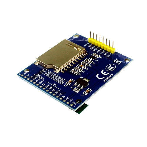
1, drilling parameters: the setting of drilling parameters is crucial, drilling speed is too fast back the drill bore force is too large and broken, drilling speed is too slow will reduce production efficiency. Because the PCB board thickness, copper thickness, plate structure and other conditions of the PCB board produced by the board manufacturer are not the same, the PCB needs to be set according to the specific situation. Through calculation and testing, the most suitable drilling parameters are selected. Generally, such as 0.3mm drill, the cutting speed should be 1.5-1.7m/min, and the drilling depth should be controlled between 0.5-0.8. 2, the cushion plate, aluminum drilling plate requirements moderate hardness, uniform thickness, flat, thickness difference should not exceed 0.076mm, such as the irregular distribution of the cushion plate is easy to jam the drill, the cushion plate is not smooth, will make the foot of the pressure is not strict, is the drill nozzle twisted bre
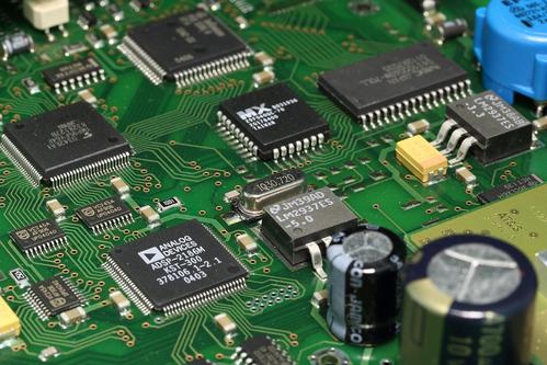
1. Prevent burrs and scratches on the surface of PCB board. 2, heat dissipation and drill cleaning function. 3, can guide the drill into the track of the PCB board to improve the accuracy of drilling. Aluminum sheet requires a large thermal conductivity, so that the heat generated during drilling can be quickly taken away, reduce the temperature of the drill, should try to use 0.15-0.2mm thick aluminum sheet or 0.15-0.35mm aluminum alloy composite aluminum sheet, effectively prevent drilling due to the high temperature caused by poor drilling chip removal and resulting in broken drill. 3, the quality of the copper clad sheet material, the glass fiber cloth of the sheet material is thick, the binding force is not good, and it will also have a greater impact on the drill break. If the resin polymerization of the plate is not complete, it is easy to produce more glue residue of the hole wall, poor chip discharge and broken drill. If there are holes in the substrate, the drill nozz
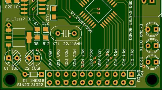
1) The diameter of the test pad specially used for detection should not be less than 0.9mm. 2) The space around the test pad should be greater than 0.6mm and less than 5mm. If the height of the component is greater than 6.7mm, the test pad shall be placed 5mm away from the component. 3) Do not place any components or test pads within 3mm of the edge of the printed circuit board. 4) The test pad should be placed in the center of a 2.5mm hole in a grid. If possible, allow the use of a standard probe and a more reliable fixture. 5) Do not rely on the edge of the connector pointer for pad testing. The gold-plated pointer is easily damaged by the test probe. 6) Avoid plating through holes - probes on both sides of the printed circuit board. Place the test tip through the hole on the non-component/weld side of the printed circuit board.
Inquiry Now

