 +86 755 2794 4155
  sales@knownpcb.com
-
Shenzhen KNOWNPCB Technology Co., Ltd.
 +86 755 2794 4155
  sales@knownpcb.com
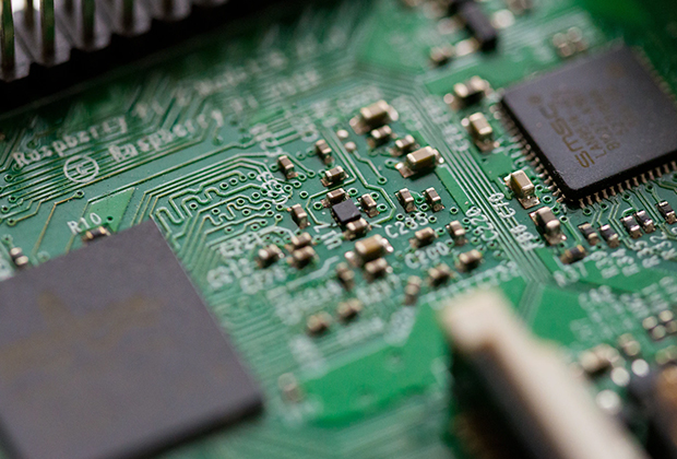
Have you noticed that now more and more of our lighting is using led lighting.What is LED? Compared to the traditional light bulbs, LEDs have lower power consumption, longer lifetime and higher energy efficiency. In the PCB industry,when we say LED PCB, it refers to the pcb used for LED lighting, if you are looking for a suitable LED PCB for your lighting system, this article may bring you something. WHAT ARE LEDS COMPOSED OF?LED is an initial light-emitting diode that produces light when an electric current passes through. LEDs typically have negative and positive electrodes, which generate light in the visible light region.The LEDS are glued to the PCB by soldering process and have electrical connections for lighting.Since light-emitting diodes dissipate a lot of heat when they are in use, when you are designing LED, the metal core is usually the best choice for LED PCB, it is because that it dissipates heat more faster. Among them, the metal material aluminum is the most widely used
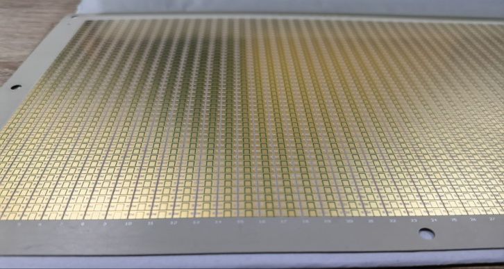
The high frequency board application such as 5G, routers, bluetooth headsets and other products that require fast signal transmission frequency. KnownPCB engaged in varies high frequency material, such as RO4003C, RO4350B,RO3006,RO5880....etc. The following is the DK value for reference. It is our big advantage in new material and high technology update.We can provide a variety of different types boards to meet your needs. No matter prototype 1pcs or mass production. Contact us now for further more info.
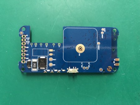
1) Double-head ultraviolet drilling system; 2) Double-head CO2 laser drilling system; 3) Hybrid laser drilling system (CO2 and UV). Such drilling systems in all HDI PCB board fabrication processes have their own advantages and disadvantages. Laser drilling systems can be simply divided into two types, two-bit single-wavelength systems and two-bit dual-wavelength systems. Regardless of the type, there are two main components that affect the ability to drill: 1) Laser energy/pulse energy; 2) Beam positioning system. The energy of the laser pulse and the transmission efficiency of the beam determine the drilling time, which refers to the time for the laser drilling machine to drill a micro-through hole, and the beam positioning system determines the speed of movement between the two holes. These factors together determine the laser drilling mechanism for the given requirements of the micro-hole speed. The dual-head UV laser system is best suited for drilling holes smalle
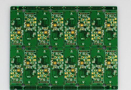
When we open the keyboard of a general-purpose computer, we see a soft film (flexible insulating substrate) printed with a silver-white (silver paste) conductive pattern and a health pattern. Because of the general screen printing method to obtain this pattern, we call this printed circuit board flexible silver paste printed circuit board. And we go to the computer city to see a variety of computer host board, graphics cards, network cards, modems, sound cards and household appliances on the printed circuit board is different. The substrate used is made of paper base (usually used for single side) or glass cloth base (often used for double side and multi-layer), pre-pregassed phenolic or epoxy resin, one or both surface layers are glued to a copper-coated sheet and then laminate and cure. This circuit board covered with copper sheet plate, we call it a rigid plate. Then made into a printed circuit board, we call it a rigid printed circuit board. Single-sided printed circuit graphic
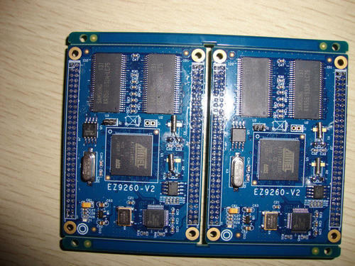
1. Poor wear resistance, the wear resistance said here is not the wear resistance of metal materials, which refers to the PCB surface ink in use will often be worn off causing blurring, fading and so on. 2. Aesthetic requirements, the appearance of the metal surface printing feels relatively low-end, which is not suitable for some products with relatively high appearance requirements, such as commemorative badges, metal business cards, exquisite company promotional nameplates, handicraft description nameplates, etc., which cannot meet their appearance requirements. 3. Ordinary printing process requires the use of organic solvents and heavy metal elements and other chemical raw materials, these substances have certain toxicity and will cause personal injury to the screen printing staff, in addition, the drying process of screen printing ink, volatile chemical raw materials gradually volatilized into the air, causing pollution to the air and the environment. Compared with traditio
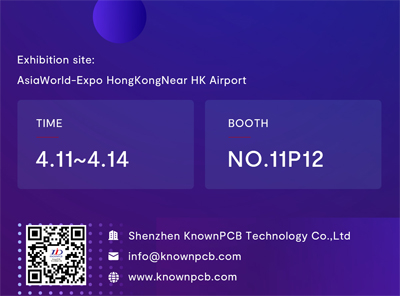
KnownPCB will attend Global Sourcing Electronics Exhibition in AsiaWorld-Expo,HongKong on Apr.11-14,2024.The address is at Asia Expo, Hongkong Asia expo, Booth No.: 11P12.We sincerely invite you to visit our Booth 11P12 in HK then.

Water-based cleaning process is based on water as the cleaning medium, in order to improve the cleaning effect, a small amount of surfactants, washing additives, corrosion inhibitors and other chemicals can be added to the water (the general content is 2%-10%). And can be in accordance with the specific situation of different nature of pollution on the printed circuit board, in the water-based cleaning agent additives, so that the scope of application of cleaning is wider. Water-based cleaning agent has a good dissolution effect on water-soluble dirt, and then with heating, brushing, spraying, ultrasonic cleaning and other physical cleaning means, can achieve better cleaning effect. The addition of surfactant to the water-based cleaning agent can greatly reduce the surface tension of water, strengthen the penetration and spreading ability of the water-based cleaning agent, and better penetrate into the gap between the closely arranged electronic components, and clean the dirt that
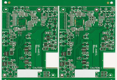
1. Dimensional stability of incoming substrate materials, especially the dimensional consistency between each laminating CYCLE of the supplier; Even if the dimensional stability of different cycles of the substrate of the same specification is within the specification requirements, due to the poor consistency between them, the graphic size of the subsequent mass production of the plate is out of line due to the difference between different batches of plate materials after the first plate trial production has determined a reasonable inner layer compensation. At the same time, there is a material anomaly that the board is found to shrink in the process of the outer pattern transfer to the shape process; In the production process, it was found that the width of the panel and the length of the shipping unit had a serious contraction in relation to the outer pattern transfer ratio during the pre-shape processing data measurement process, and the ratio reached 3.6mil/10inch. The specific
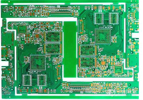
Step 1 Drill holes The design of the through hole aperture below 8mil, the hole spacing is close, plus each board about 500,000 to 1.2 million blind holes, the hole deviation and plugging of the through hole, and the perforation of the perforation will affect the PCB yield. Drilling machine needs to be maintained according to the regulations, the use of appropriate aluminum sheet and drill nozzle, in the production of new materials engineers to confirm the rationality of the operation parameters: number of sheets, tool parameters, etc. The amount of dust suction of the drilling machine needs to meet the standard, and the drilling needle has space for debris removal is also crucial. The pass shape and aperture, dielectric thickness, material and laser energy of the laser are very important, and it is necessary to set the best operating conditions. Step 2: Electroplating Electroplated copper carries the functions of current conduction and signal transmission, and the electroplating
Inquiry Now

