 +86 755 2794 4155
  sales@knownpcb.com
-
Shenzhen KNOWNPCB Technology Co., Ltd.
 +86 755 2794 4155
  sales@knownpcb.com
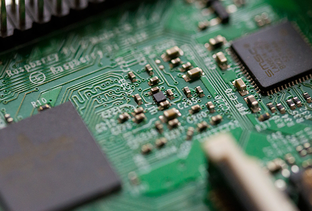
Have you noticed that now more and more of our lighting is using led lighting.What is LED? Compared to the traditional light bulbs, LEDs have lower power consumption, longer lifetime and higher energy efficiency. In the PCB industry,when we say LED PCB, it refers to the pcb used for LED lighting, if you are looking for a suitable LED PCB for your lighting system, this article may bring you something. WHAT ARE LEDS COMPOSED OF?LED is an initial light-emitting diode that produces light when an electric current passes through. LEDs typically have negative and positive electrodes, which generate light in the visible light region.The LEDS are glued to the PCB by soldering process and have electrical connections for lighting.Since light-emitting diodes dissipate a lot of heat when they are in use, when you are designing LED, the metal core is usually the best choice for LED PCB, it is because that it dissipates heat more faster. Among them, the metal material aluminum is the most widely used
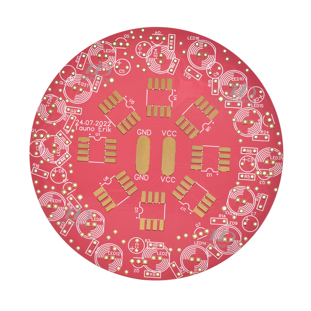
1. Hot air leveling (tin spraying) Hot air leveling, also known as hot air solder leveling (commonly known as tin spraying), is a process of coating the surface of a PCB with molten tin (lead) solder and flattening it with heated compressed air, forming a coating layer that is not only resistant to copper oxidation but also provides good solderability. Hot air leveling forms copper tin intermetallic compounds at the junction of solder and copper. PCB should sink into the melted solder during hot air leveling; The wind knife blows out the liquid solder before it solidifies; The wind knife can minimize the crescent shape of the solder on the copper surface and prevent solder bridging. 2. Organic Solderability Protector (OSP) OSP is a process for surface treatment of copper foil on printed circuit boards (PCBs) that complies with RoHS instructions. OSP is the abbreviation for Organic Solderability Preservatives, which is translated as organic solder mask, also known as copper prote
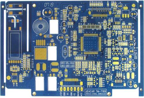
1. Issues related to substrate processing: Especially for some thinner substrates (usually below 0.8mm), due to poor substrate rigidity, it is not suitable to use a brush machine to brush the board. This may not effectively remove the protective layer specially treated to prevent oxidation of the copper foil on the surface of the substrate during production and processing. Although this layer is thin and easy to remove by brushing, chemical treatment poses significant difficulties. Therefore, it is important to pay attention to control during production and processing to avoid poor bonding between the substrate copper foil and chemical copper, which may cause foaming on the surface of the substrate; When blackening is carried out on thin inner layers, there may also be problems such as poor blackening and browning, uneven color, and poor local blackening and browning. 2. The phenomenon of poor surface treatment caused by oil stains or other liquids contaminated with dust during
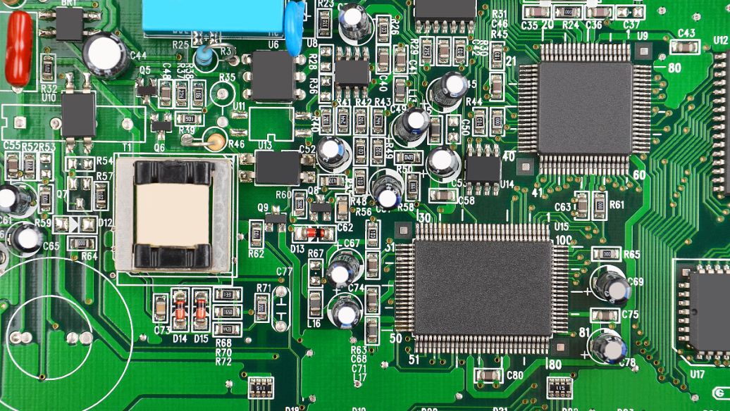
If you want to produce circuit boards that do not contain halogen elements, you need to start with the raw materials. According to the JPCA-ES-01-2003 standard, copper clad boards with chlorine (C1) and bromine (Br) content less than 0.09% Wt (weight ratio) are defined as halogen-free copper clad boards. (Meanwhile, the total amount of CI+Br is ≤ 0.15% [1500PPM]). So why ban brine? Halogens refer to halogen elements in the periodic table of chemical elements, including fluorine (F), chlorine (CL), bromine (Br), and iodine (1). At present, flame retardant substrates such as FR4 and CEM-3 are mostly brominated epoxy resins as flame retardants. In brominated epoxy resin, tetrabromobisphenol A, polybrominated biphenyls, polybrominated biphenyl ethers, and polybrominated diphenyl ethers are the main blocking fuels for copper clad laminates, with low cost and compatibility with epoxy resin. However, research by relevant institutions has shown that flame retardant materials containing ha
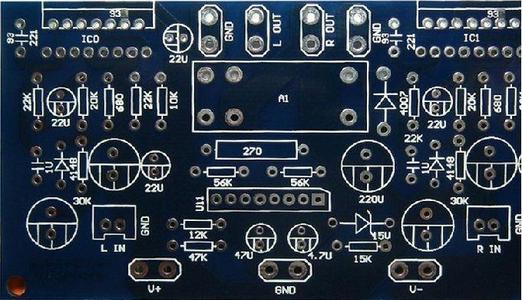
1. The resistance generated by alternating current on components is related to capacitance and inductance. When an electronic signal waveform is transmitted in a conductor, the resistance it experiences is called impedance. 2. Resistance is the resistance generated by direct current on components, which is related to voltage, resistivity, and current. Application of characteristic impedance 1. The electrical performance provided by printed circuit boards for high-speed signal transmission and high-frequency circuits must be able to prevent reflection during signal transmission, maintain signal integrity, reduce transmission losses, and play a matching role. Only in this way can complete, reliable, accurate, worry free, and noise free transmission signals be obtained. 2. The size of impedance cannot be simply understood as better or better, the key is matching. Control parameters of characteristic impedance
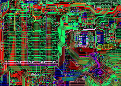
1. Bubbles There are bubbles generated between the lines or on the side of a single line on an FPC printed board after development. Main reasons: The formation of bubbles between two or more lines is mainly due to the narrow spacing between the lines and the high height of the lines. During screen printing, the solder mask cannot be printed on the substrate, resulting in the presence of air or moisture between the solder mask and the substrate. During curing and exposure, the gas expands due to heating, causing a single line to be mainly caused by the high height of the line. When the scraper contacts the line, the line is too high, and the angle between the scraper and the line increases, making it impossible for the solder mask to be printed on the root of the line. This causes gas to exist between the side of the line root and the solder mask layer, and after heating, bubbles are generated. The solution is to visually inspect whether the solder mask is completely printed on the

1. The effect of reducing temperature on the stress of PCB boards Since temperature is the main source of stress on the board, reducing the temperature of the reflow furnace or slowing down the heating and cooling rate of the board in the reflow furnace can greatly reduce the occurrence of bending and warping of the board. However, there may be other side effects, such as solder short circuits. 2. Using high Tg boards Tg is the glass transition temperature, which is the temperature at which a material transitions from a glass state to a rubber state. The lower the Tg value of a material, the faster its board begins to soften after entering the reflow furnace, and the longer it takes to become a soft rubber state, the more severe the deformation of the board. Using a higher Tg board can increase its ability to withstand stress and deformation, but the cost of the material is relatively high. 3. Increase the thickness of the circuit board Many electronic products, in order to ac
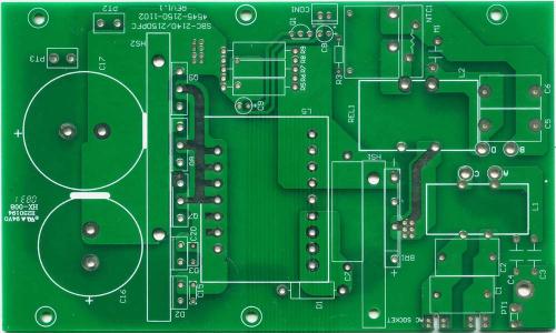
Poor solderability of circuit board holes will result in virtual soldering defects, affecting the parameters of components in the circuit, leading to unstable conduction of multi-layer board components and inner wires, and causing the entire circuit function to fail. The so-called weldability refers to the property of the metal surface being wetted by molten solder, that is, the formation of a relatively uniform and continuous smooth attached film on the metal surface where the solder is located. The main factors affecting the solderability of printed circuit boards are: (1) the composition of the solder and the properties of the soldered material. Solder is an important component of the welding chemical treatment process, which is composed of chemical materials containing flux. The commonly used low melting point eutectic metals are Sn-Pb or Sn-Pb-Ag. The impurity content should be controlled in a certain proportion to prevent the oxide produced by impurities from being dissolve
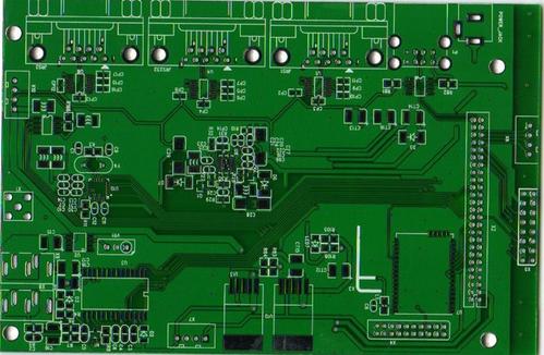
1. Problem: Decreased etching rate in printed circuits Reason: Caused by improper control of process parameters Solution: Inspect and adjust process parameters such as temperature, spray pressure, solution density, pH value, and ammonium chloride content to the specified values according to process requirements. 2. Problem: Deposition of etching solution in printed circuits Reason: (1) The ammonia content is too low (2) Excessive water dilution (3) The specific gravity of the solution is too high Solution: (1) Adjust the pH value to reach the process specified value or appropriately reduce the exhaust volume. (2) Strictly follow the process requirements or reduce the exhaust volume appropriately during adjustment. (3) According to the process requirements, a portion of the solution with high specific gravity is discharged and analyzed, and then an aqueous solution of ammonium chloride and ammonia is added to adjust the specific gravity of the etching solution to the al
Inquiry Now

