 +86 755 2794 4155
  sales@knownpcb.com
-
Shenzhen KNOWNPCB Technology Co., Ltd.
 +86 755 2794 4155
  sales@knownpcb.com
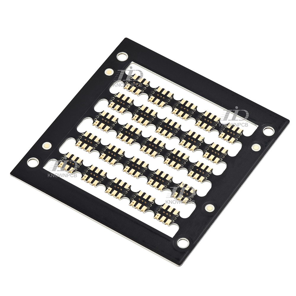
Have you noticed that now more and more of our lighting is using led lighting.What is LED? Compared to the traditional light bulbs, LEDs have lower power consumption, longer lifetime and higher energy efficiency. In the PCB industry,when we say LED PCB, it refers to the pcb used for LED lighting, if you are looking for a suitable LED PCB for your lighting system, this article may bring you something. WHAT ARE LEDS COMPOSED OF?LED is an initial light-emitting diode that produces light when an electric current passes through. LEDs typically have negative and positive electrodes, which generate light in the visible light region.The LEDS are glued to the PCB by soldering process and have electrical connections for lighting.Since light-emitting diodes dissipate a lot of heat when they are in use, when you are designing LED, the metal core is usually the best choice for LED PCB, it is because that it dissipates heat more faster. Among them, the metal material aluminum is the most widely used
There are certain technical requirements for the rate of copper deposition when using a chemical copper plating solution. If the speed is too slow, it may cause voids or pinholes in the hole wall; If the copper deposition rate is too fast, it will result in rough coating. Therefore, scientific determination of copper deposition rate is one of the means to control the quality of copper deposition. Taking the example of the chemical plating of thin copper provided by Xianling, briefly introduce the method for measuring the copper deposition rate: (1) Material: Using epoxy substrate after copper etching, with a size of 100 x 100 (mm). (2) Measurement steps: A. Bake the sample at 120-140 ℃ for 1 hour, and then weigh W1 (g) using an analytical balance; B. Corrosion in a mixture of 350-370 grams/liter of chromic anhydride and 208-228 milliliters/liter of sulfuric acid (at a temperature of 65 ℃) for 10 minutes, then rinse with clean water; C. Treat the waste liquid from chromium removal
In general, the distribution of copper foil on PCB circuit boards is very complex and difficult to accurately model. Therefore, when modeling, it is necessary to simplify the shape of the wiring and make ANSYS models as close as possible to the actual circuit board. The electronic components on the circuit board can also be simulated using simplified modeling, such as MOS transistors, integrated circuit blocks, etc. Thermal analysis Thermal analysis in SMT processing can assist designers in determining the electrical performance of components on PCB circuit boards, helping them determine whether components or circuit boards will burn out due to high temperatures. Simple thermal analysis only calculates the average temperature of the circuit board, while complex ones require establishing transient models for electronic devices containing multiple circuit boards. The accuracy of thermal analysis ultimately depends on the accuracy of the component power consumption provided by the c
To obtain the accurate cause or mechanism of PCB failure or defect, basic principles and analysis processes must be followed. Otherwise, valuable failure information may be missed, resulting in the inability to continue the analysis or the possibility of obtaining incorrect conclusions. The general basic process is to first determine the failure location and mode based on the failure phenomenon through information collection, functional testing, electrical performance testing, and simple visual inspection, that is, failure localization or fault localization. For simple PCBs or PCBAs, it is easy to determine the location of failure. However, for more complex BGA or MCM packaged devices or substrates, defects are not easy to observe through a microscope and cannot be determined at the moment. In this case, other means need to be used to determine. Next, it is necessary to analyze the failure mechanism, using various physical and chemical methods to analyze the mechanisms that cause

With the development of electronic products towards high density and precision, the same requirements have been put forward for circuit boards. The most effective way to increase PCB density is to reduce the number of through holes and precisely set blind holes and buried holes to achieve this. 1. Definition of blind holes a: Compared to through holes, through holes refer to holes that are drilled through each layer, while blind holes are non drilled through holes. (Illustrated, eight layer board examples: through hole, blind hole, buried hole) b: blind hole subdivision: BLIND HOLE, buried hole Buried HOLE (outer layer not visible); c: Distinguish from the production process: blind holes are drilled before pressing, while through holes are drilled after pressing. 2. Production method A: Diamond belt: (1) : Select reference point: Select a through hole (i.e. a hole in the first drilling strip) as the unit reference hole. (2) Each blind hole drill belt needs to select a hole an
OSP is the abbreviation for Organic Solderability Preservatives, also known as copper protector. Simply put, OSP is a chemical method that grows a layer of organic film on a clean bare copper surface. This film has oxidation resistance, heat resistance, impact resistance, and moisture resistance, used to protect the copper surface of circuit boards from oxidation or vulcanization in normal environments; But in the subsequent welding high temperature, this protective film must be easily removed by the flux quickly, so that the exposed clean copper surface can immediately combine with the molten solder to form a solid solder joint in a very short time. 1. Process flow: degreasing → water washing → micro etching → water washing → acid washing → pure water washing → OSP → pure water washing → drying. 2. Principle: A layer of organic film is formed on the copper surface of the circuit board, firmly protecting the fresh copper surface and preventing oxidation and pollution even at high
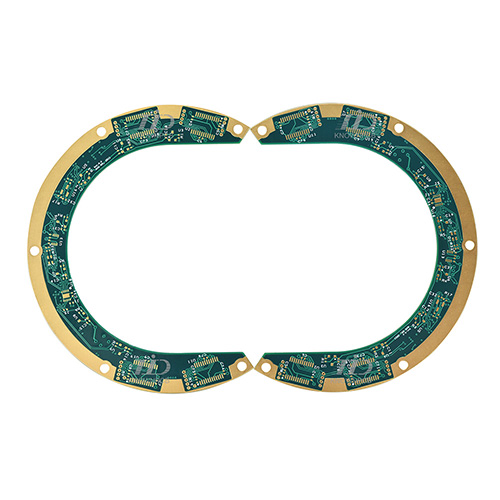
To solve the above problems of gold-plated boards, PCBs using gold-plated boards mainly have the following characteristics: 1. Due to the different crystal structures formed by gold deposition and gold plating, gold deposition will appear more yellow than gold plating, resulting in better customer satisfaction. 2. Due to the different crystal structures formed by sinking gold and plating gold, sinking gold is easier to weld than plating gold, and will not cause welding defects, leading to customer complaints. 3. Due to the fact that only nickel gold is present on the solder pad of the sinking gold plate, the signal transmission in the skin effect is in the copper layer and will not affect the signal. 4. Due to the denser crystal structure of deposited gold compared to gold plating, it is less prone to oxidation. 5. Due to the fact that only nickel gold is present on the solder pad of the sinking gold plate, it will not produce gold wire and cause slight shortening.
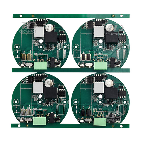
1. Annual maintenance knowledge: 1. Clean the dust on the circuit board. 2. The electrolytic capacitor capacity in the circuit board is randomly checked, if the capacity of the electrolytic capacitor is found to be less than 20% of the nominal capacity, it should be replaced, and the general life of the electrolytic capacitor should be replaced for about ten years to ensure the working performance of the pcb. 3. For high-power devices coated with heat dissipation silicone grease, check whether the heat dissipation silicone grease is dry and solid. For dry and solid devices, remove the dry and solid heat dissipation silicone grease and apply new heat dissipation silicone grease to prevent the high-power devices in the circuit board from burning out due to poor heat dissipation. 2, seasonal maintenance: 1. Clean the dust on the circuit board every quarter, use the circuit board special cleaning solution for cleaning, after cleaning the dust above, dry the circuit board with a ha
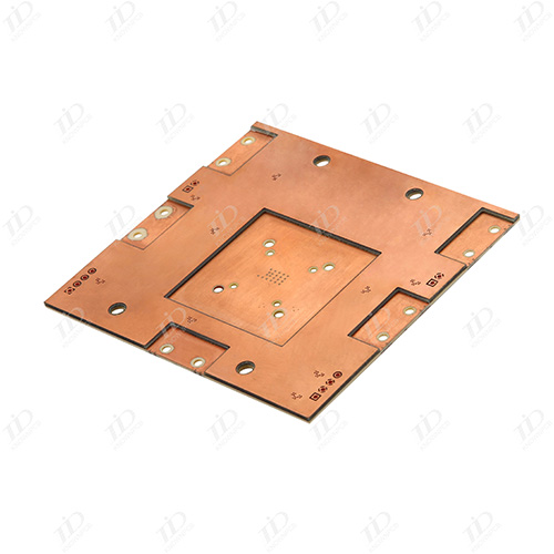
First, the different materials used in flexible circuit boards cause the diversity of prices Taking ordinary double panels as an example, the board material is generally PET, PI, etc., the board thickness ranges from 0.0125mm to 0.10mm, and the copper thickness ranges from 0.0125mm to 0.10mm. Oz to 3 Oz, all of which creates a huge price difference in sheet metal alone; The different brands of materials also have a certain price difference, so the different materials cause the diversity of prices. Second, the different production processes used in flexible circuit boards cause the diversity of prices Different production processes result in different costs. Such as gold-plated plate and tinned plate, the accuracy of the production shape, the use of silk screen lines and dry film lines will form different costs, leading to the diversity of prices. Third, the price diversity caused by the different difficulty of the flexible circuit board itself Even if the material is the same
Inquiry Now

