 +86 755 2794 4155
  sales@knownpcb.com
-
Shenzhen KNOWNPCB Technology Co., Ltd.
 +86 755 2794 4155
  sales@knownpcb.com
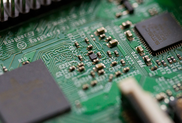
Have you noticed that now more and more of our lighting is using led lighting.What is LED? Compared to the traditional light bulbs, LEDs have lower power consumption, longer lifetime and higher energy efficiency. In the PCB industry,when we say LED PCB, it refers to the pcb used for LED lighting, if you are looking for a suitable LED PCB for your lighting system, this article may bring you something. WHAT ARE LEDS COMPOSED OF?LED is an initial light-emitting diode that produces light when an electric current passes through. LEDs typically have negative and positive electrodes, which generate light in the visible light region.The LEDS are glued to the PCB by soldering process and have electrical connections for lighting.Since light-emitting diodes dissipate a lot of heat when they are in use, when you are designing LED, the metal core is usually the best choice for LED PCB, it is because that it dissipates heat more faster. Among them, the metal material aluminum is the most widely used
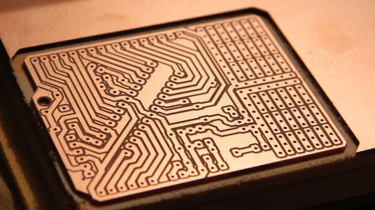
1. There are various problems that occur in the PCB process, and process engineers often take on the responsibility of forensic autopsy (analysis of the causes of defects and solutions) Therefore, the main purpose of initiating this discussion question is to discuss one by one in the equipment area, including personnel, machinery, materials, and possible problems that may arise under certain conditions 2. Processes that use pre-treatment equipment, such as inner pre-treatment lines, electroplating copper pre-treatment lines, D/F, solder mask (solder mask) Wait a minute 3. Taking the pre-treatment line for solder mask (solder mask) on hard board PCB as an example (different manufacturers may have differences): brush grinding * 2 groups ->water washing ->acid washing ->water washing ->cold air knife ->drying section ->sun disk collection ->discharge collection 4. Generally, steel brushes with brush wheels of # 600 and # 800 are used, which can affect the roughness of the board sur
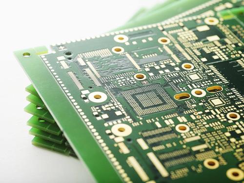
The first step is to obtain a PCB, and first record the models, parameters, and positions of all the components on paper, especially the direction of diodes, transistors, and IC notches. It is best to take two photos of the position of the pneumatic components with a digital camera; Step 2, remove all components and remove the tin from the PAD holes. Clean the PCB with alcohol, then put it into the scanner, start POHTOSHOP, scan the silk screen surface in color, and print it out for later use; Step three, use gauze paper to lightly polish the top layer and bottom layer until the copper film is shiny. Place them in the scanner, start Photoshop, and scan the two layers in color. Note that the PCB must be placed horizontally and straight in the scanner, otherwise the scanned image cannot be used. Please select a scanner resolution of 600; Step four, adjust the contrast and brightness of the canvas to make the parts with and without copper film more contrasting. Then, turn the secon

The original size of the copper-clad board is too large, making it inconvenient to process. Sometimes, it cannot even be placed in the printed circuit board processing equipment for processing. Therefore, it is necessary to first cut it into several copper-clad boards of different processing sizes. As for the specific size of the processing size, it needs to be determined based on the processing equipment for producing printed circuit boards, the size of each printed circuit board, and some process parameters. These process parameters not only include the length and width required for the printed circuit graphics themselves, but also the width consumed for fixing the screw holes on the printed circuit board to the electronic product frame, the process allowance for external processing, the clamping allowance for fixtures during chemical plating, electroplating, and corrosion, the positioning pin allowance for multi-layer printed circuit boards, the alignment mark allowance between

1. The assembly density of multi-layer circuit boards is high and their volume is small. With the decreasing volume of electronic products, higher requirements are also put forward for the electrical performance of PCBs, and the demand for multi-layer circuit boards is also increasing. 2. The use of multi-layer circuit boards facilitates wiring, significantly shortens the length of wiring, and shortens the connections between electronic components, which also improves the speed of signal transmission. 3. For high-frequency circuits, after adding a ground layer, the signal line will form a constant low impedance to the ground, resulting in a significant reduction in circuit impedance and better shielding effect. 4. For electronic products with high heat dissipation requirements, multi-layer circuit boards can be equipped with metal core heat dissipation layers, which is convenient to meet special functional needs such as shielding and heat dissipation. In terms of performance, m
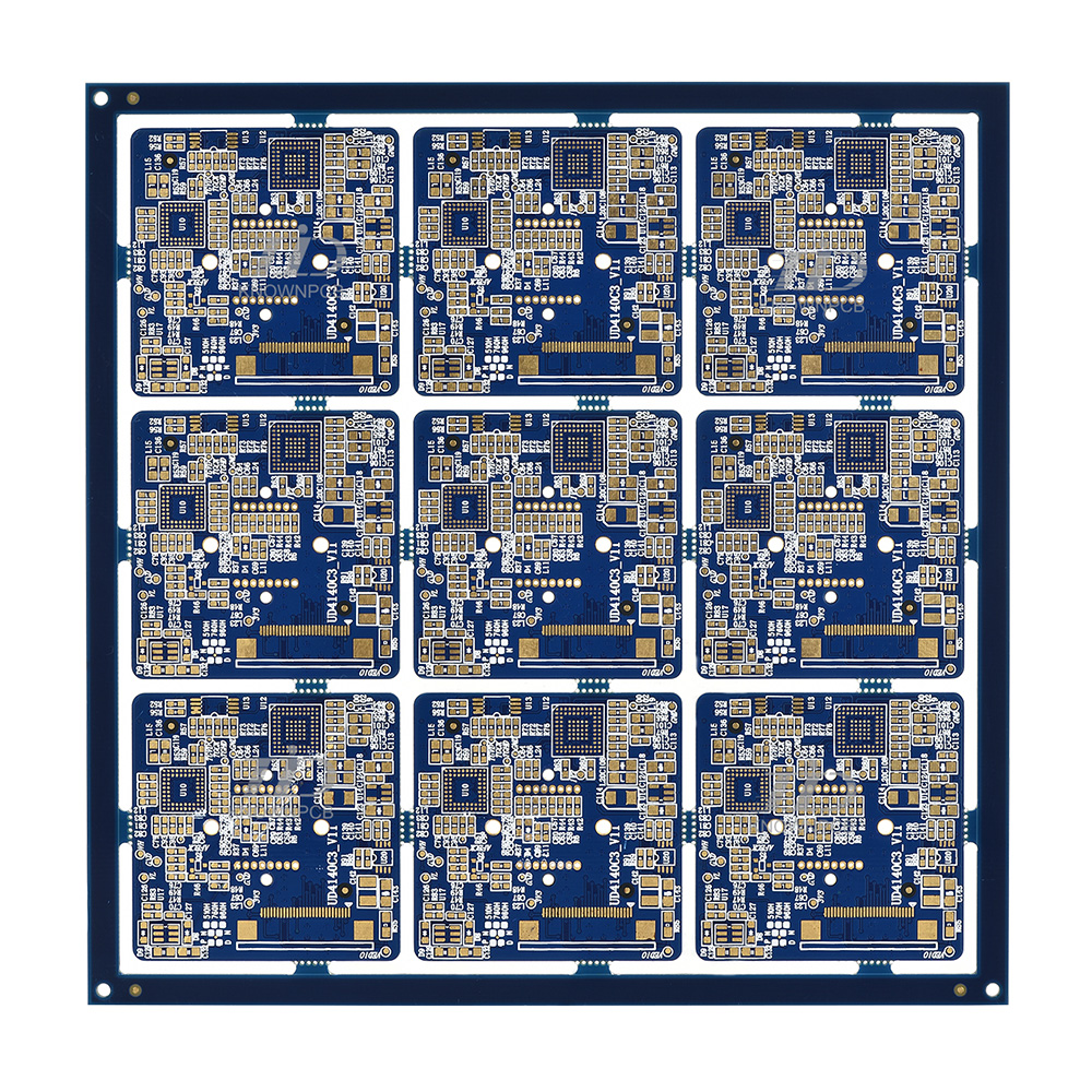
1. Drilling parameters: The setting of drilling parameters is crucial. If the drilling speed is too fast, the drilling nozzle will break due to excessive force, and if the drilling speed is too slow, it will reduce production efficiency. Due to differences in the thickness, copper thickness, and material structure of PCB boards produced by various board manufacturers, PCBs need to be set according to specific circumstances. Select the most suitable drilling parameters through calculation and testing. Generally, for a 0.3mm drill bit, the cutting speed should be between 1.5-1.7m/min, and the drilling depth should be controlled between 0.5-0.8. 2. The cushion plate used for drilling aluminum sheets requires a moderate hardness, uniform thickness, flatness, and a thickness difference of no more than 0.076mm. If the distribution of the cushion plate's softness and hardness is irregular, it is easy to get stuck in the drilling nozzle. If the cushion plate is uneven, it will cause the p

At present, there are four types of flexible circuits: single-sided, double-sided, multi-layer flexible boards, and rigid flexible boards. ① Single sided flexible board is the lowest cost printed board when it does not require high electrical performance. When wiring on one side, a single-sided flexible board should be selected. It has a layer of chemically etched conductive patterns, and the conductive pattern layer on the flexible insulation substrate surface is rolled copper foil. The insulation substrate can be polyimide, polyethylene terephthalate, aramid fiber ester, and polyvinyl chloride. ② Double sided flexible board is a conductive pattern made by etching one layer on each side of the insulating substrate film. Metallized holes connect the patterns on both sides of the insulating material to form a conductive path, in order to meet the design and functional requirements of flexibility. And the covering film can protect single and double-sided wires and indicate the posi
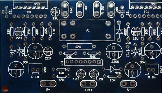
At present, 5G is booming, and with the arrival of the 5G era, PCB, as the mother of the electronic industry and the carrier of all components, occupies the largest proportion and benefits the PCB industry in this chain. The development of 5G cannot do without the construction of large-scale data centers, which will inevitably increase the number of servers. The development of servers cannot do without PCBs. Due to the huge traffic carried by data centers and the high requirements for transmission speed, the requirements for the number of layers and materials of PCBs will also become higher. In this case, the demand for high-end communication boards will be greatly increased. With the continuous advancement of 5G construction, due to the high-speed and high-frequency characteristics of 5G, the value of communication boards for a single base station will also be greatly increased, and the demand for communication boards in 5G base station construction will be further stimulated. F
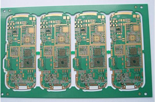
1. Engineering design: The arrangement of interlayer semi cured sheets should correspond; Multi layer core boards and semi cured sheets should use the same supplier's products; The area of the outer C/S surface graphics should be as close as possible, and independent grids can be used; 2. Drying the board before cutting Generally, at 150 degrees Celsius for 6-10 hours, the moisture inside the board is eliminated to further solidify the resin completely and eliminate stress inside the board; Bake the board before cutting, whether it is the inner layer or both sides! 3. Attention should be paid to the warp and weft directions of the cured sheets before laminating the multi-layer board: The contraction ratio in the warp and weft directions is different. Before cutting and stacking the semi cured sheet, pay attention to distinguishing the warp and weft directions; When cutting the core board, attention should also be paid to the warp and weft directions; The general direction of th
Inquiry Now

