 +86 755 2794 4155
  sales@knownpcb.com
-
Shenzhen KNOWNPCB Technology Co., Ltd.
 +86 755 2794 4155
  sales@knownpcb.com
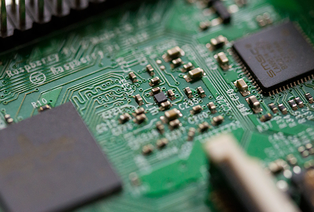
Have you noticed that now more and more of our lighting is using led lighting.What is LED? Compared to the traditional light bulbs, LEDs have lower power consumption, longer lifetime and higher energy efficiency. In the PCB industry,when we say LED PCB, it refers to the pcb used for LED lighting, if you are looking for a suitable LED PCB for your lighting system, this article may bring you something. WHAT ARE LEDS COMPOSED OF?LED is an initial light-emitting diode that produces light when an electric current passes through. LEDs typically have negative and positive electrodes, which generate light in the visible light region.The LEDS are glued to the PCB by soldering process and have electrical connections for lighting.Since light-emitting diodes dissipate a lot of heat when they are in use, when you are designing LED, the metal core is usually the best choice for LED PCB, it is because that it dissipates heat more faster. Among them, the metal material aluminum is the most widely used
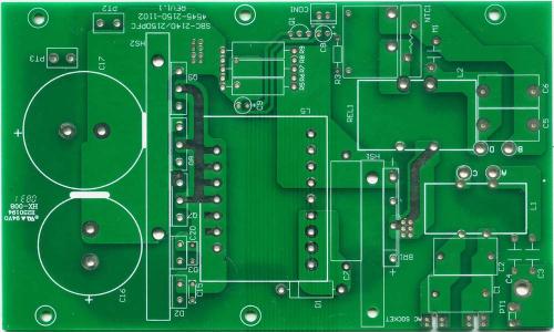
In almost all electronic products, printed circuit boards (PCBs) are an indispensable core component, known as the heart of electronic products. The performance and quality of PCBs directly affect the reliability, operational efficiency, and service life of electronic devices. Firstly, PCB provides a physical platform for all components in electronic devices, ensuring efficient flow of current between different components through precise layout and design, thereby ensuring the normal operation of the equipment. Secondly, as electronic products develop towards smaller, lighter, and thinner directions, PCBs are also constantly evolving. High density interconnect (HDI) technology and multi-layer board design enable more electronic components to be integrated into smaller spaces, meeting the needs of miniaturization. Once again, the design and manufacturing process of PCBs require high precision and rigorous quality control. Excellent PCB design can reduce electromagnetic interferen
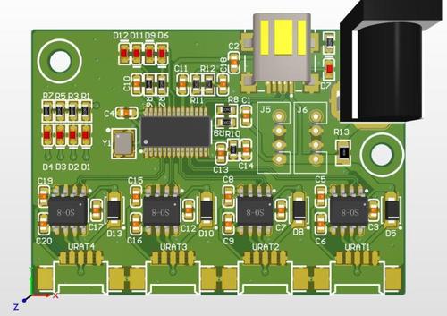
Printed Circuit Board (PCB) is a bridge connecting the electronic world. Through precise circuit and interface design, various components in electronic devices can work together to create a rich and colorful digital life. Firstly, the basic function of a PCB is to provide a platform for electronic signals to flow and exchange between different components. On this platform, numerous components such as microprocessors, memory, sensors, etc. can communicate and collaborate through predefined paths. Secondly, with the diversification and complexity of electronic devices, PCB design has become increasingly complex. From simple single-layer boards to complex multi-layer boards, and even three-dimensional packaging, the design and manufacturing technology of PCBs has been constantly improving. Once again, with the development of emerging technologies such as the Internet of Things, artificial intelligence, and 5G, the PCB industry is facing new challenges and opportunities. The progres

Copper coating refers to using the idle space on the PCB as a reference plane and then filling it with solid copper. These copper areas are also known as copper filling. The significance of copper plating is to reduce the impedance of the ground wire and improve its anti-interference ability; Reduce voltage drop and improve power efficiency; Also, connect to the ground wire to reduce the loop area. If there is a lot of ground on a PCB, such as SGND, AGND, GND, etc., how to cover it with copper? My approach is to use the most important "ground" as a reference for independent copper plating based on the different positions of the PCB board, and to separate the digital and analog copper plating without much explanation. Before copper plating, first thicken the corresponding power lines: V5.0V, V3.6V, V3.3V (SD card power supply), and so on. In this way, multiple deformation structures with different shapes are formed. There are several issues that need to be addressed in copper plati

PCB surfaces are generally coated with a layer of paint to protect the metal, and the paint should be removed before recycling. There are two types of paint removers: organic paint removers and alkaline paint removers. Organic paint removers have high toxicity and pose great harm to human health and the environment, while alkaline paint removers have relatively low toxicity. We obtained the optimal formula for paint removal through experiments: place the cut PCB chips into a 10% sodium hydroxide solution. Adding 0.5% additive A, 0.5% additive B, and 0.05% corrosion inhibitor mercaptobenzotriazole, heating in a water bath can completely remove the surface paint within 30 minutes, further recovering the exposed metal. Alkaline paint stripping is the separation of paint from the contact area of the circuit board. The paint mainly exists in its original structure and can be recycled.
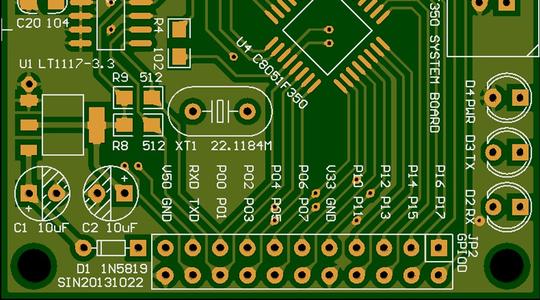
Physical methods for PCB recycling and processing The physical method involves recycling based on differences in physical properties such as material density, conductivity, magnetism, and surface wettability. The main processes include disassembly, crushing, sorting, recovery of precious metals, and treatment of harmful substances. (1) The general order of selective dismantling of electronic waste is to select reusable parts. Disassemble harmful components and classify parts of various materials. The disassembly methods include manual disassembly, mechanical disassembly, and automatic disassembly. The automatic disassembly of PCBs uses methods such as bath washing or hot air heating to dissolve solder, and then uses vacuum clamps or robots to remove surface components of PCBs. (2) Broken. The crushing of PCB includes impact crushing, extrusion crushing, and shear crushing. The most successful application currently is the ultra-low temperature freezing crushing technology, which ca
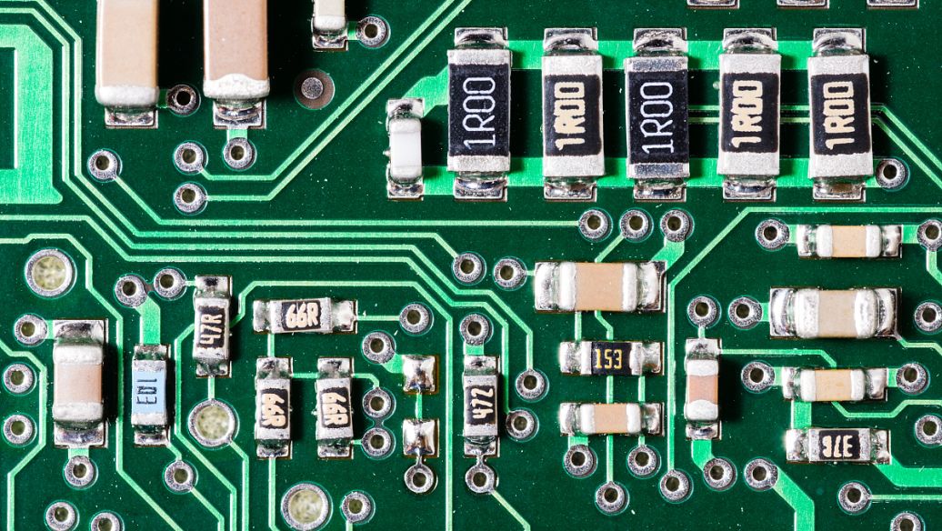
1. There are various problems that occur during the PCB manufacturing process, and process engineers often take on the responsibility of forensic autopsy (analysis of the causes of defects and solutions). The main purpose is to discuss the potential issues that may arise in terms of personnel, machinery, materials, and conditions in the equipment area one by one. We hope that everyone can participate and provide their own opinions and opinions. 2. Processes that use pre-treatment equipment, such as inner pre-treatment lines, electroplating copper pre-treatment lines, D/F, solder mask (solder mask) Wait a minute. 3. Taking the pre-treatment line for solder resistance (solder mask) of hard board PCB as an example (different manufacturers may have differences): brush grinding * 2 groups ->water washing ->acid washing ->water washing ->cold air knife ->drying section ->sun disk collection ->discharge collection. 4. Generally, steel brushes with brush wheels of # 600 and # 800 are us

Symptoms: Poor adhesion of printing materials, poor adhesion of coatings, inability to etch off certain parts, and inability to solder certain parts. Possible inspection methods: Visual inspection is usually performed by forming visible water marks on the surface of the board: Possible reason: Due to the extremely dense and smooth surface caused by the demolding film, the uncoated copper surface becomes excessively bright. Usually, on the uncoated side of the laminate, the laminate manufacturer does not remove the release agent. The pinholes on the copper foil cause resin to flow out and accumulate on the surface of the copper foil, which usually occurs on copper foils thinner than 3/4 ounce weight specifications. Copper foil manufacturers apply excess antioxidants to the surface of copper foil. The manufacturer of the laminated board has changed the resin system, demoulding thin, or brushing method. Due to improper operation, there are many fingerprints or oil stains. Stain eng
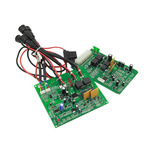
The assembly of electronic products poses significant challenges to production scheduling due to the large number and variety of components, as well as the short lifespan of electronic products. Multi variety, small batch, and variable batch production have become the mainstream production mode in electronic manufacturing. In this mode, the switching time between multiple varieties occupies an increasingly large proportion of the entire assembly time. Composed of a high-speed SMT machine and a multifunctional SMT machine. In fact, the entire PCB assembly line also includes equipment such as feeding machines, screen printing machines, dispensing machines, reflow soldering and curing furnaces, and take-up machines. These devices are connected in series to form the PCB assembly line, but these auxiliary devices do not constitute the bottleneck process of the entire assembly line, so they are omitted during modeling. Each SMT machine can accommodate 20 feeding slots, and each componen
Inquiry Now

