 +86 755 2794 4155
  sales@knownpcb.com
-
Shenzhen KNOWNPCB Technology Co., Ltd.
 +86 755 2794 4155
  sales@knownpcb.com
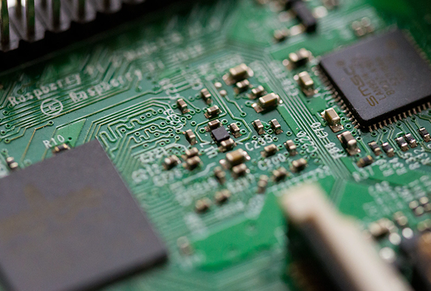
Have you noticed that now more and more of our lighting is using led lighting.What is LED? Compared to the traditional light bulbs, LEDs have lower power consumption, longer lifetime and higher energy efficiency. In the PCB industry,when we say LED PCB, it refers to the pcb used for LED lighting, if you are looking for a suitable LED PCB for your lighting system, this article may bring you something. WHAT ARE LEDS COMPOSED OF?LED is an initial light-emitting diode that produces light when an electric current passes through. LEDs typically have negative and positive electrodes, which generate light in the visible light region.The LEDS are glued to the PCB by soldering process and have electrical connections for lighting.Since light-emitting diodes dissipate a lot of heat when they are in use, when you are designing LED, the metal core is usually the best choice for LED PCB, it is because that it dissipates heat more faster. Among them, the metal material aluminum is the most widely used
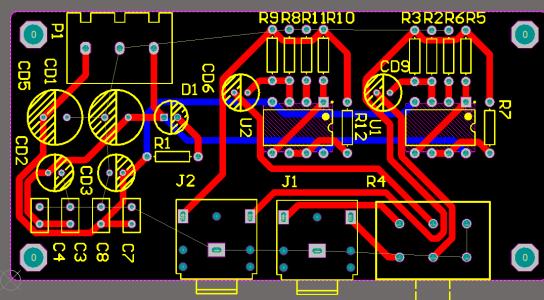
The purpose of tin plating on PCB circuit boards is to prevent bare copper from reacting directly with oxygen in the air, causing oxidation of the board surface. In addition, tin plating is also helpful for PCBA surface mounting, which can be directly melted and used for plug-in, accelerating welding efficiency. So what is the reason for the PCB circuit board not being soldered? Let's take a look below. There are several reasons why PCB boards are not soldered: 1. PCB circuit board oxidation, PCB board not tin coated. 2. The temperature of the furnace is too low or the speed is too fast, and the tin has not melted. 3. If there is a solder paste issue, you can try changing to another type of solder paste. 4. The most common issue with battery cells is that they are usually made of stainless steel and require electroplating with a layer of chromium before tin can be applied. If there is oil or poor electroplating on this electroplating layer, it may not be able to solder. You ca
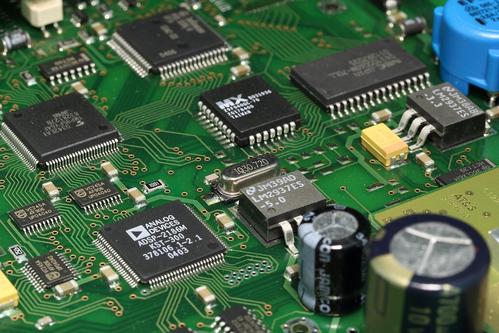
It is generally believed that if the frequency of a digital logic circuit reaches or exceeds 45MHz~50MHz, and the circuit operating above this frequency already occupies a certain proportion of the entire electronic system (such as 1/3), it is called a high-speed circuit. In fact, the harmonic frequency at the edge of the signal is higher than the frequency of the signal itself, which is an unexpected result of signal transmission caused by the rapid changes in the rising and falling edges (also known as signal jumps) of the signal. Therefore, it is generally agreed that if the line propagation delay is greater than 1/2 of the rise time of the digital signal driver end, such signals are considered high-speed signals and generate transmission line effects. The transmission of signals occurs at the moment when the signal state changes, such as the rise or fall time. The signal passes through a fixed period of time from the driving end to the receiving end. If the transmissio
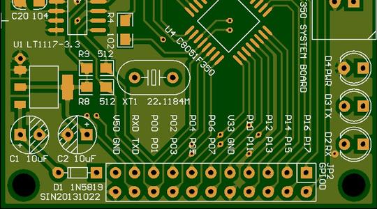
Principle 1: Look first, measure later The circuit board to be repaired should first be visually inspected. If necessary, a magnifying glass should also be used for observation. Mainly looking at: 1. Are there any broken wires or short circuits; Especially whether there is any breakage or adhesion in the connecting wires of the printed circuit board; 2. Whether there is disconnection phenomenon in relevant components such as resistors, capacitors, inductors, diodes, and transistors; Has anyone repaired it? What components have been touched? Is there any problem of virtual welding, missing welding, reverse insertion, or incorrect insertion. After ruling out the above conditions, first use a multimeter to measure the resistance value between the power supply and ground of the circuit board. Generally, the resistance value of the circuit board should not be less than 70 Ω. If the resistance value is too small, it is only a few or ten ohms. This indicates that there are component
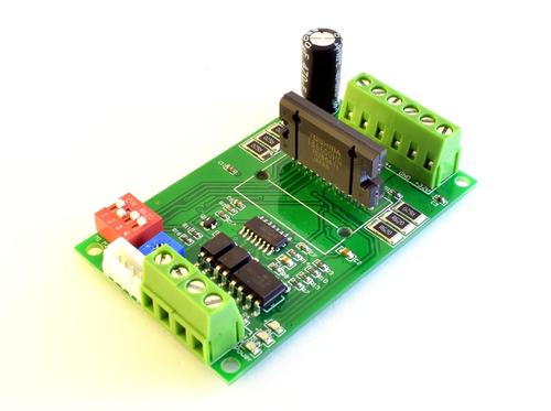
(1) Pre drying The purpose of pre drying is to evaporate the solvent contained in the ink and make the solder mask non stick. The pre drying temperature and time vary depending on the type of ink. Excessive pre drying temperature or prolonged drying time can lead to poor development and reduced resolution; If the pre drying time is too short or the temperature is too low, the film will adhere during exposure. During development, the solder mask film will be corroded by sodium carbonate solution, causing the surface to lose luster or the solder mask film to expand and fall off. (2) Exposure Exposure is the key to the entire process. For positive images, when overexposed, due to light scattering, the solder mask at the edges of the pattern or line reacts with light (mainly the photosensitive polymers contained in the solder mask react with light), generating residual film and reducing the resolution, resulting in a smaller developed pattern and thinner lines; If exposed When insu
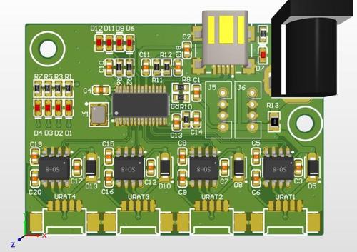
1. Film negatives should not have problems such as trachoma or scratches. When placing, the film surface should be facing upwards and should not rub against other objects. When copying, the film surface should be operated on. After use, it should be promptly placed in a suitable film bag for storage. 2. When aligning, the film should be facing the board. When taking the film, use both hands to pick it up diagonally and avoid touching other objects to avoid scratching the film surface. When each film reaches a certain number of boards, stop aligning and have a dedicated person inspect or replace it. After use, put it in a suitable film bag for storage. 3. Operators are not allowed to wear any decorations such as rings, bracelets, etc. on their hands. Nails should be regularly trimmed and kept smooth, and no debris should be placed on the surface of the counter. The countertop should be kept clean and smooth. 4. Before production, it is necessary to strictly inspect the screen to
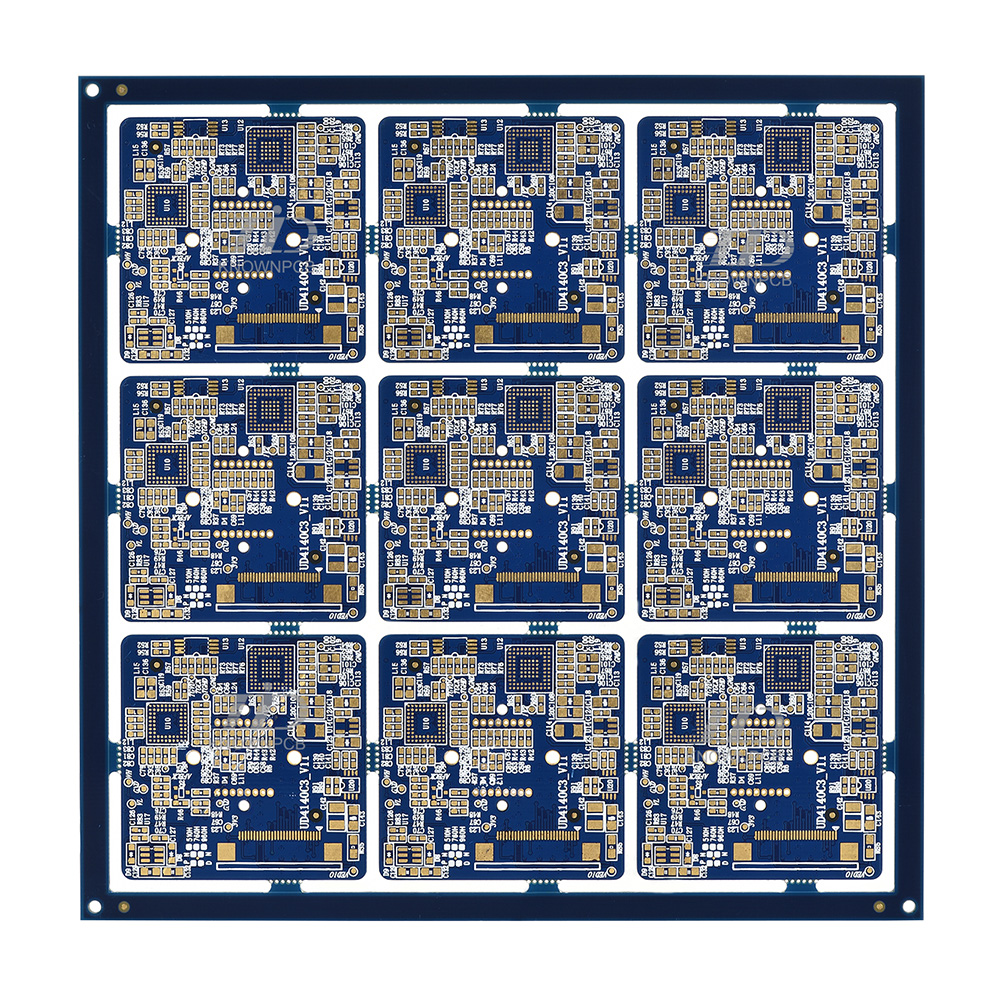
a、 According to the mechanical rigidity of copper-clad laminates, they are divided into rigid copper-clad laminates and flexible copper-clad laminates; b、 According to the insulation material and structure of copper clad laminates, they are divided into organic resin based copper clad laminates, metal based copper clad laminates, and ceramic based copper clad laminates; c、 According to the thickness of the copper clad plate, it is divided into thick plate (with a thickness range of 0.8-3.2mm (including Cu)) and thin plate (with a thickness range of less than 0.78mm (excluding Cu)); d、 According to the reinforcing materials of copper clad laminates, they are divided into glass cloth based copper clad laminates, paper based copper clad laminates, and composite based copper clad laminates (CME-1, CME-2). e、 Divided into flame retardant board and non flame retardant board according to flame retardant level. f、 According to certain properties of copper-clad laminates, they are divi
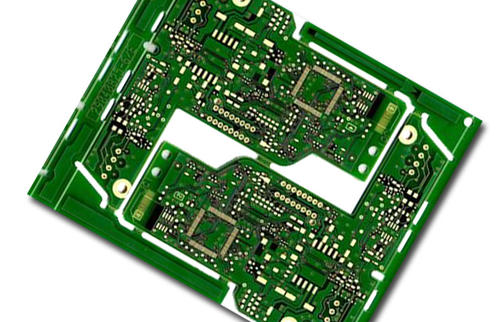
Circuit components: In order to improve the functionality of printed boards, there are now more and more printed components. In high-frequency digital circuits, wires are transmission lines with impedance requirements and are not simply conductive. There are also inductors, resistors, capacitors, etc. printed on the board surface or buried inside the board. (2) Reliability: withstands certain environmental conditions and has a certain service life. Environmental conditions: The product will definitely be used under certain temperature, humidity, air pressure, and environmental gas conditions. The indoor temperature of the TV, the gas in the refrigerator and kitchen, the electronic instruments of the car are exposed to ice and snow (negative 45 degrees Celsius) and the scorching heat of the desert (positive 60 degrees Celsius), and the communication equipment of the ship is affected by dampness and salt mist in harsh weather conditions. Printed boards may be subjected to these env
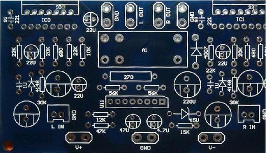
To exceed the limits of the extreme working conditions listed in the manual. All idle inputs on the device must be connected to VDD or VSS and have good contact. All low impedance devices (such as pulse signal generators, etc.) are connected to CMOS or NMOS integrated circuit inputs All MOS integrated circuits (including P-channel MOS, N-channel MOS, complementary MOS-CMOS integrated circuits) have an insulating gate to prevent voltage breakdown. The thickness of the insulation gate oxide layer in general devices is approximately 25nm, 50nm, and 80nm. In front of the high impedance gate of the integrated circuit, there is a resistor diode network for protection. However, the protection network inside the device is not sufficient to avoid electrostatic damage (ESD) to the device. Experiments have shown that the device will fail during high voltage discharge, and the device may also fail due to the accumulation of multiple lower voltage discharges. There are various forms of electr
Inquiry Now

