 +86 755 2794 4155
  sales@knownpcb.com
-
Shenzhen KNOWNPCB Technology Co., Ltd.
 +86 755 2794 4155
  sales@knownpcb.com
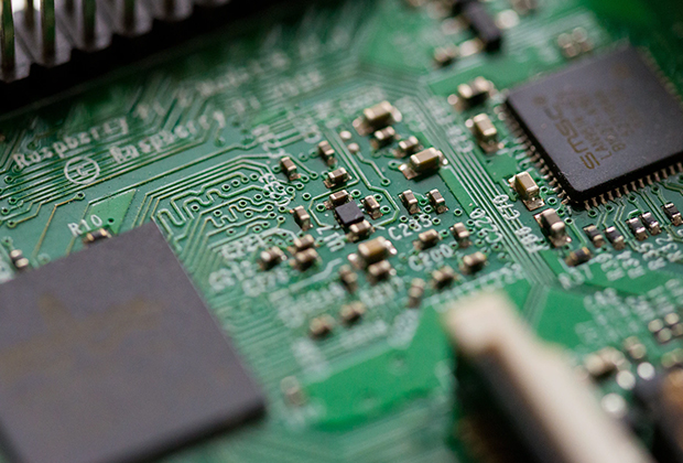
Have you noticed that now more and more of our lighting is using led lighting.What is LED? Compared to the traditional light bulbs, LEDs have lower power consumption, longer lifetime and higher energy efficiency. In the PCB industry,when we say LED PCB, it refers to the pcb used for LED lighting, if you are looking for a suitable LED PCB for your lighting system, this article may bring you something. WHAT ARE LEDS COMPOSED OF?LED is an initial light-emitting diode that produces light when an electric current passes through. LEDs typically have negative and positive electrodes, which generate light in the visible light region.The LEDS are glued to the PCB by soldering process and have electrical connections for lighting.Since light-emitting diodes dissipate a lot of heat when they are in use, when you are designing LED, the metal core is usually the best choice for LED PCB, it is because that it dissipates heat more faster. Among them, the metal material aluminum is the most widely used
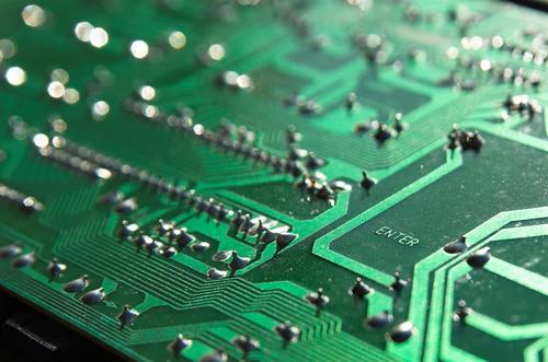
1: The process flow of selective welding includes: flux spraying, circuit board preheating, immersion welding, and drag welding. The flux coating process plays an important role in selective welding. When welding is heated and completed, the flux should have sufficient activity to prevent bridging and oxidation of the circuit board. The flux spraying is carried by an X/Y robotic arm above the flux nozzle on the circuit board, Spray flux onto the soldering position of the double-sided circuit board. 2: The most important aspect of microwave peak selection welding after reflow soldering is accurate flux spraying. Micro hole spraying will never contaminate the area outside the solder joint. Micro point spraying has a minimum flux point pattern diameter greater than 2mm, so the precision of the flux position deposited on the circuit board is ± 0.5mm to ensure that the flux always covers the soldered area. 3: The process characteristics of selective soldering can be understood by comp
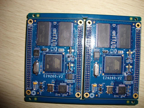
Among them, the most common four layer PCB board thickness in Tongling is 1.6mm, and four layer boards above 3.0mm are relatively rare. Customized 0.6-3.5mm thick PCB boards are supported. The four layer board lamination diagram shows that for a 1.6mm thick PCB, the top layer is 1 ounce of copper, followed by a (0.2mm-0.5oz) thick PP sheet, followed by a second signal layer with a copper foil thickness of only 0.5 ounces, followed by a (1.2mm-0.5OZ) thick core layer, and the bottom layer is a 0.2mm thick PP sheet, Finally, there is a 1 ounce bottom layer. The 6-layer board is similar. PP sheet and core board: Prepregs are thin insulation materials for PCBs. Prepregs, also known as pre impregnated materials, are mainly used as adhesive and insulating materials for the inner conductive patterns of multi-layer printed boards before being laminated. After being laminated, the semi cured epoxy resin is squeezed out, begins to flow and solidify, bonding the multi-layer circuit boards to
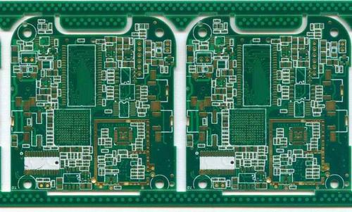
The so-called ceramic circuit board is a type of thermal conductive organic ceramic circuit board prepared using thermal conductive ceramic powder and organic adhesive, with a thermal conductivity coefficient of 9-20W/m.k under conditions below 250 ℃. Ceramic circuit boards are mainly used in areas such as high voltage, high insulation, high frequency, high temperature, high reliability, and small volume electronic products. 1. High precision clock oscillator, voltage controlled oscillator, temperature compensated oscillator ceramic circuit board. 2. Metallization of ceramic substrates for refrigerators. 3. Metallization of ceramic substrates for surface mounted inductors. Metallization of Inductive Magnetic Core Electrodes. 4. High insulation and high voltage ceramic circuit board for power electronic control modules. 5. Ceramic circuit boards for high-temperature circuits in oil wells. 6. Solid state relay ceramic circuit board. 7. DC-DC module power supply ceramic circui
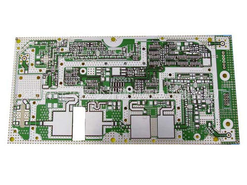
With the continuous updating and upgrading of electronic products, new products have entered thousands of households. However, many friends are not very clear about the production process of PCB sampling factories when they first start planning PCBs, and do not know what line width is more suitable. Below, the editor will based on Professional PCB manufacturers are constantly updating and upgrading their electronic products, and new products have entered millions of households. However, many friends are not very clear about the production process capability of PCB manufacturers when they first plan their PCBs, and do not know what line width is suitable. Below, the editor will provide specific explanations based on the factory's production capability. 1. The width of the primary PCB power line should be above 40 mils, and the width should also be above 25 mils if conditions permit; 2. Other considerations also include practical current. Generally, 10mil can withstand a large curre
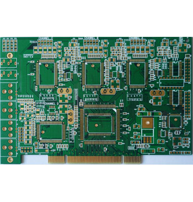
1. Board thickness: 0.8, 1.0, 1.2, 1.6, 2.0 are commonly used standards. If there are no special requirements, choose a board thickness of 1.6mm. 2. Copper foil thickness: 0.5, 1.0, 2.0 are commonly used standards. If the power is not particularly high, it is not necessary to choose a board. Manufacturers usually use a board with a power of 0.5oz. If the power is around 100W, a board with a power of 1.0 or higher will be used. 3. The colors for solder mask: green, black, red, and white are commonly used. If there are no specific requirements, green should be used. If you are using it for your own experiment, green should be used even more, as this color is the clearest for circuit boards. 4. Solder pad treatment: sinking gold, anti oxidation, tin spraying (divided into lead and lead-free), generally using the latter two can be used, and the storage time of tin spraying will be longer. 5. Screen printing colors: White and black are commonly used colors. If it is green oil, white
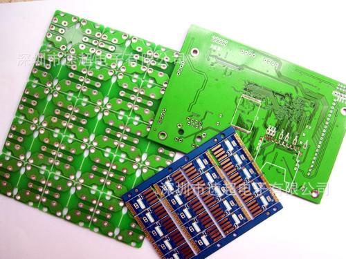
Generally, the thickness of copper foil (covered with copper) for single and double-sided PCB boards is about 35um (1.4mil), while another specification is 50um and 70um. The thickness of the surface layer of the multi-layer board is generally 35um=1oz (1.4mil), and the inner layer is 17.5um (0.7mil). 70% of circuit boards are used to achieve a copper foil thickness of 35um, which mainly depends on the use of the PCB and the size of the signal voltage and current; In addition, for PCBs that require excessive current, some may use 70um copper thickness, 105um copper thickness, and very rarely 140um copper thickness, etc. The thickness of copper foil is usually expressed in oz (ounces), which refers to the thickness of copper uniformly covered by 1oz of copper on an area of 1 square foot, which is approximately 1.4 mils. It is expressed in terms of weight per unit area to indicate the uniform thickness of copper foil. Use a formula to indicate that 1oz=28.35g/FT2 (FT2 is square feet
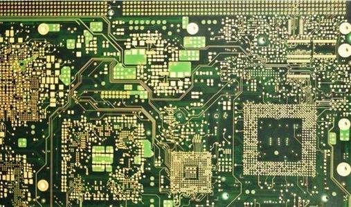
With the continuous updating and replacement of electronic products, from single panel to double-sided board, it can be said that the development is rapid. PCB is known as the "mother of electronic products", and almost all electronic products cannot do without PCB. There are also more and more new products. With the continuous updating and replacement of electronic products, from single panel to double-sided board, it can be said that the development is rapid. PCB is known as the "mother of electronic products", and almost all electronic products cannot do without PCB. There are also more and more new products, and more new products represent There is a constant demand for testing samples, but some cases are quite urgent. When making samples, we will choose urgent ones. So, what is the price of 24-hour urgent PCB sampling? Let me explain in detail below. Common Sense of 24-hour Urgent PCB Sample Prices for Direct Sales by Manufacturers In this era of money, it is the right cho
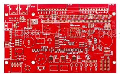
PCB sampling manufacturers generally refer to electronic products being sent to the circuit board manufacturer for processing into circuit boards for inspection after the engineer completes the PCB layout design. Due to being a newly developed product, many functions are still incomplete, and there are still many functional requirements for debugging. Only after debugging is qualified can batch production be carried out. If debugging is not qualified, it is necessary to modify, sample, and debug again, reducing many unnecessary troubles in the later stage. With the increasingly fierce market competition, price issues have become a concern for buyers. The characteristic of PCB sample prices is that they change according to the quantity and delivery time of the samples. Generally speaking, a typical single and double-sided board is not urgent, with a quantity of less than 10 pieces and a standard process within 100 * 100mm. Generally, it only costs 50 yuan. However, if your quantity i
Inquiry Now

