 +86 755 2794 4155
  sales@knownpcb.com
-
Shenzhen KNOWNPCB Technology Co., Ltd.
 +86 755 2794 4155
  sales@knownpcb.com
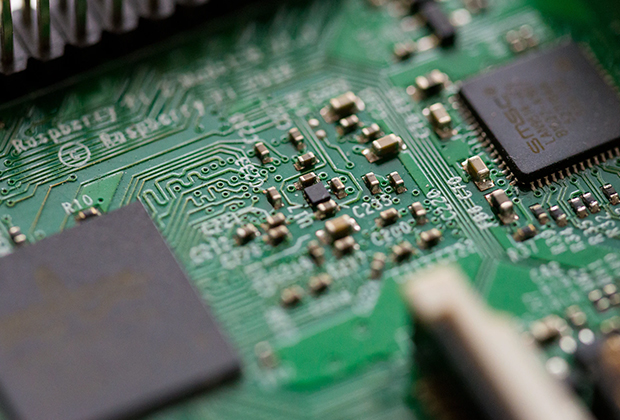
Have you noticed that now more and more of our lighting is using led lighting.What is LED? Compared to the traditional light bulbs, LEDs have lower power consumption, longer lifetime and higher energy efficiency. In the PCB industry,when we say LED PCB, it refers to the pcb used for LED lighting, if you are looking for a suitable LED PCB for your lighting system, this article may bring you something. WHAT ARE LEDS COMPOSED OF?LED is an initial light-emitting diode that produces light when an electric current passes through. LEDs typically have negative and positive electrodes, which generate light in the visible light region.The LEDS are glued to the PCB by soldering process and have electrical connections for lighting.Since light-emitting diodes dissipate a lot of heat when they are in use, when you are designing LED, the metal core is usually the best choice for LED PCB, it is because that it dissipates heat more faster. Among them, the metal material aluminum is the most widely used
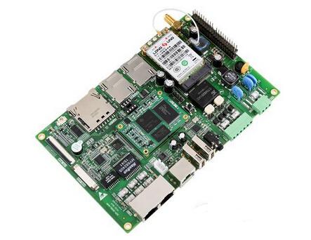
In commercial production, there are two laser technologies available for laser drilling. The wavelength of CO2 laser is in the far-infrared band, and the wavelength of ultraviolet laser is in the ultraviolet band. CO2 laser is widely used in the production of industrial micro through-holes on printed circuit boards, with a requirement that the diameter of the micro through-hole be greater than 100 μ (Raman, 2001). For the production of these large aperture holes, CO2 laser has high productivity because the punching time required for CO2 laser to produce large holes is very short. UV laser technology is widely used in diameters less than 100 μ In the production of micro pores in m, with the use of miniaturized circuit diagrams, the pore size can even be less than 50 μ M. Ultraviolet laser technology in the production of diameters less than 80 μ The yield of m holes is very high. Therefore, in order to meet the increasing demand for microporous productivity, many manufacturers have b
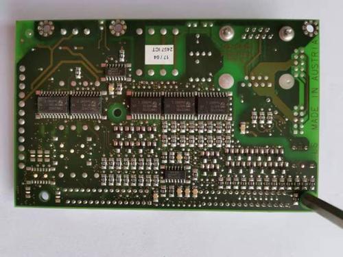
CO2 laser effectively removes dielectrics, even non-uniform glass reinforced dielectrics. However, a single CO2 laser cannot create small holes (less than 75 μ m) In addition to removing copper, Suzhou circuit board sample manufacturers believe that there are also a few exceptions, which are that it can remove pre processed 5 μ Thin copper foil below m (Lustino, 2002). UV laser can create very small holes and remove all ordinary copper streets (3-36 μ m. 1oz, even electroplated copper foil. UV laser can also remove dielectric materials separately, but at a slower speed. Moreover, for non-uniform materials, such as reinforced glass FR-4, the effect is usually not good. This is because only when the energy density is increased to a certain extent can the glass be removed, which will also damage the inner solder pads. Due to the fact that the stick laser system includes ultraviolet laser and CO2 laser, it can achieve better results in both fields. UV laser can complete all copper foil
1. Report the results of the work The leader who lifts the heavy weight is the favorite. When reporting work, please remember to report the result to the leader first, and the result thinking is the first thinking. 2. Ask for work plan Please ensure that at least two programs are given to leaders, and express their views and effective suggestions. Don't let the leader do the quiz questions, but let the leader do the multiple-choice questions. Don't ask the leader how to do this thing, what to do, but ask, I have a plan, you can listen to it and see how it goes! 3. Summarize the work process and find three points To do a work summary, it is necessary to describe the process, not only to have a clear sequence and logic, but also to find out the key points, mistakes, and reflection points in the process. 4. Arrange work standards and clarify customer requirements Layout work must be clear about customer requirements and quality standards, otherwise subordinates will not know ho
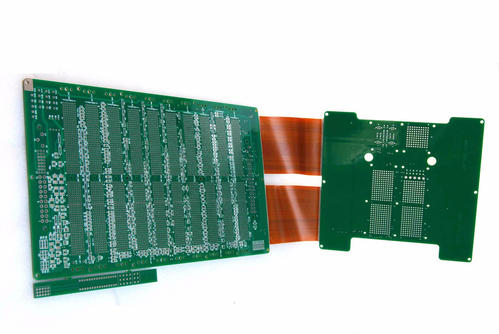
After the customer's plug-in test, it is found that the via hole (via hole) is not connected. The test can be carried out normally before the plug-in, and the appearance has no drilling deviation phenomenon, which is mainly caused by the following five reasons: First: the hole copper is not enough; Second: the roughness of the hole wall is too large Third: Drilling dust plug holes Fourth: drilling broken knife to make up holes Fifth: poor solder mask plug hole In terms of controlling the problem of through-hole failure, the hole copper is the most important link. The automatic sinking copper line of our Honglian circuit is not small: Detection: The detection method of immersion copper wire is mainly backlight series detection. The number of series is more than 9 to be qualified to ensure the quality of copper immersion and hole formation. The detection methods include deposition speed force detection (copper layer thickness in standard time); glue removal speed force (this
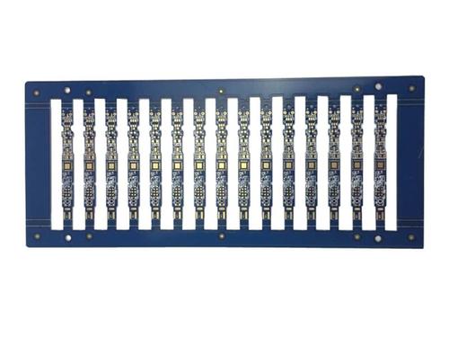
One, circuit board factory tin surface quality defects So what are the factors that cause the bad tin surface of the tin surface? According to the analysis of the editor, there are the following points 1. The operation is not in accordance with the operating specifications when shipping The circuit industry has extremely strict requirements on the workshop environment and the standard operation of employees, especially the chemical reaction environment is required in the circuit board production process, so the infiltration of impurities is not allowed. After the board spraying process is completed, the subsequent one All series require employees to wear anti-static gloves to operate, because finger sweat or stains directly contact the surface, which will cause surface oxidation. If it causes defects, it is extremely difficult to find, and it is irregular, and it is difficult to be exposed in testing and tinning experiments. 2. The tin furnace for spraying tin is not cleaned on
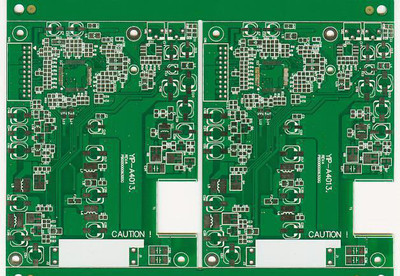
However, due to fierce market price competition, the cost of circuit board prototype materials is also on the rise. More and more manufacturers are monopolizing the market with low prices in order to enhance their core competitiveness. However, behind these ultra-low prices, they are obtained by reducing material and process manufacturing costs. However, devices are often prone to cracks (cracks), scratches, (or abrasions), and their precision, performance, and other comprehensive factors are not up to standard, seriously affecting the solderability and reliability of products used. Facing the diverse types of circuit board samples on the market, identifying the quality of circuit board samples can be approached from two aspects; One method is to judge based on appearance, and the other is to judge based on the quality specifications of the PCB board itself. 1. Standard rules for size and thickness. The thickness of a circuit board is different from that of a standard circuit boar
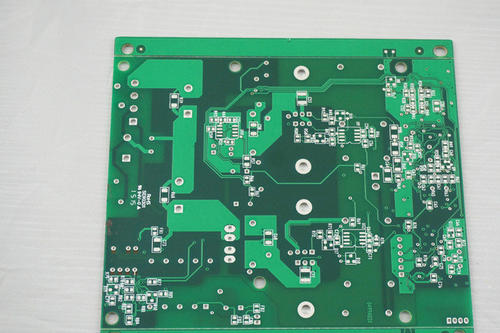
The price of PCB has always been a confusing issue for many buyers, and many people may wonder how these prices are calculated when placing orders online. Below, PCB sample manufacturers will discuss the composition factors of PCB prices together. 1. The diversity of prices caused by different materials used in PCBs. For example, ordinary double-sided boards generally have FR4 (Shengyi, Jiantao, Guoji, three prices from top to bottom), with board thicknesses ranging from 0.2mm to 3.0mm and copper thicknesses ranging from 0.5oz to 3oz, all of which cause significant price differences in board materials; In terms of solder mask ink, there is also a certain price difference between ordinary thermosetting oil and photosensitive green oil. 2. Common causes of price diversity due to different surface treatment processes include OSP (oxidation resistance), lead spray tin, lead-free spray tin (environmental protection), gold plating, gold deposition, and some combination processes, among
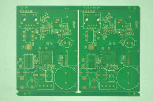
1. The issue of cleanliness of the board surface; 2. The issue of surface micro roughness (or surface energy). The blistering problem on all circuit boards can be summarized as the above reasons. Poor or too low adhesion between coatings makes it difficult to resist the coating stress, mechanical stress, and thermal stress generated during subsequent production and assembly processes, resulting in varying degrees of separation between coatings. The factors that may cause poor surface quality during the production and processing process are summarized as follows: 1. Issues with substrate processing: Especially for some thinner substrates (generally below 0.8mm), due to poor substrate rigidity, it is not suitable to use a brush machine to brush the substrate. This may not effectively remove the protective layer specially treated to prevent oxidation of the copper foil on the surface of the substrate during production and processing. Although this layer is thin and easy to remove b
Inquiry Now

