 +86 755 2794 4155
  sales@knownpcb.com
-
Shenzhen KNOWNPCB Technology Co., Ltd.
 +86 755 2794 4155
  sales@knownpcb.com
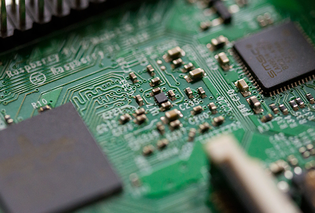
Have you noticed that now more and more of our lighting is using led lighting.What is LED? Compared to the traditional light bulbs, LEDs have lower power consumption, longer lifetime and higher energy efficiency. In the PCB industry,when we say LED PCB, it refers to the pcb used for LED lighting, if you are looking for a suitable LED PCB for your lighting system, this article may bring you something. WHAT ARE LEDS COMPOSED OF?LED is an initial light-emitting diode that produces light when an electric current passes through. LEDs typically have negative and positive electrodes, which generate light in the visible light region.The LEDS are glued to the PCB by soldering process and have electrical connections for lighting.Since light-emitting diodes dissipate a lot of heat when they are in use, when you are designing LED, the metal core is usually the best choice for LED PCB, it is because that it dissipates heat more faster. Among them, the metal material aluminum is the most widely used
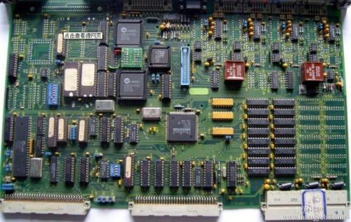
1. It is strictly prohibited to use grounded testing instruments and equipment to test the power amplifier PCB board without an isolation transformer. When coming into contact with equipment with high output power or unfamiliar with the nature of the power supply used, it is necessary to first determine whether the chassis of the machine is live, otherwise it is easy to cause a power short circuit with the live equipment on the chassis, affecting the integrated circuit, and causing the fault to expand. 2. When testing the power amplifier PCB board, attention should be paid to the insulation performance of the electric soldering iron. When testing, it is necessary to confirm that the soldering iron is not live. It is best to ground the shell of the soldering iron, and it is safer to use a low-voltage circuit iron of 6-8V. 3. It is very important to understand the working principle of integrated circuits and their related circuits before testing the power amplifier PCB board. It is
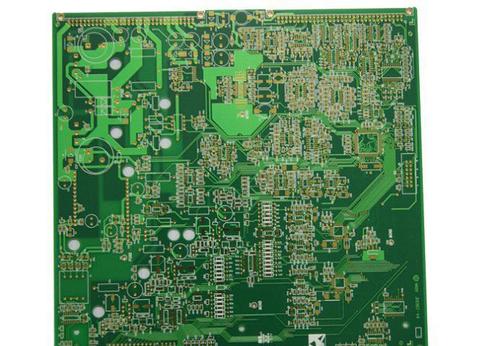
Single panel On basic medical PCB boards, the parts are concentrated on one side, while the wires are concentrated on the other side. Due to the fact that the wires only appear on one side, this type of medical PCB board is referred to as single sided. Due to the many strict restrictions on the design of a single sided circuit board (as it only has one side, the wiring cannot cross and must revolve around a separate path), only early circuits used this type of circuit board. Double-sided board This type of circuit board has wiring on both sides, but if wires are used on both sides, there should be appropriate circuit connections between the two sides. The "bridge" between these circuits is called a through hole. Through holes are small holes filled or covered with metal on medical PCB boards, which can be connected to wires on both sides. Because the area of a double-sided board is twice that of a single panel, it solves the problem of staggered wiring (which can be transmitted
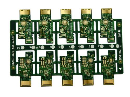
PCBA test stand is a device used to test PCBA finished products. When making PCBA test racks, PCBA processing plants usually need to provide Gerber files and PCBA samples to facilitate the production of test racks. For the current PCBA test bench, only a few pressure plate buckles are installed on the test bench, and the PCBA is fixed by a thimble and pressure plate buckle. During the PCBA function test, press the PCBA into the pressure plate buckle with both hands. Due to uneven force or insufficient compression, PCBA can easily cause poor contact between the testing needle and PCBA, seriously affecting testing efficiency and accuracy; If too much force is applied, it is easy to deform or damage the PCBA when pressing down, and it is also easy to damage the test needle of the testing frame, causing significant losses. 1、 Material preparation After determining the plan based on the information, it is necessary to prepare hardware materials (electronic components), relevant additi
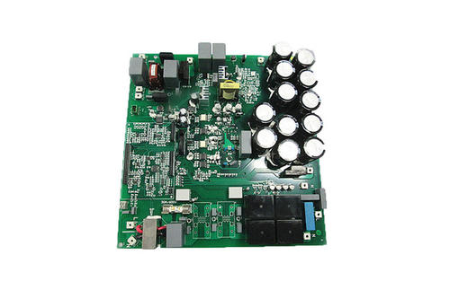
The circuit layout of HDI high-frequency boards is extremely dense, and the production price is slightly higher than that of conventional circuit boards. Only some high-end electronic products will use HDI high-frequency circuit boards, and HDI high-frequency boards include all "blind hole boards" and "buried hole boards". So, what are the differences between identifying blind hole boards and buried hole boards! ① Blind hole: refers to a through hole that connects the inner layer of the PCB to the surface layer of the PCB, but this type of hole does not penetrate the entire board. Buried hole: a through-hole that only connects the wiring between the inner layers, which cannot be seen from the surface of the PCB alone. In this regard, PCB boards with buried blind holes may not necessarily be HDI circuit boards, but HDI high-frequency boards must have blind holes. ② Taking a six layer circuit board as an example: the first/second order refers to PCB boards that require laser drilli
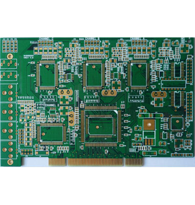
① Hole wall copper thickness: A 25 micron hole wall copper thickness effectively enhances the reliability of PCB boards and improves the Z-axis expansion resistance. ② No welding/patching repair: Perfect for no welding repair and open circuit patching repair, which can effectively ensure the reliability and safety of circuit boards. ③ IPC specifications: For some manufacturers of high-end and high-quality PCB circuit boards, exceeding IPC specifications for cleanliness can not only improve customer satisfaction and trust, but also gain a certain influence in the industry. ④ Service life: Strictly control the surface treatment of each type of PCB circuit board to ensure its solderability and reliability meet industry standards, and reduce the risk of moisture intrusion. ⑤ Substrate: According to the company's positioning standards, select internationally renowned boards to improve product reliability and known performance. ⑥ Ink: Ensure that the solder mask material used compli
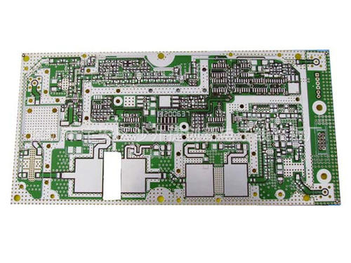
Almost all powered products cannot do without power circuit boards, but due to different application areas, there are differences in customizing power circuit boards in terms of current requirements, product specifications, surface treatment processes, and so on. Firstly, let's understand what types of power supply PCBs include: ① switching power supply ② monitoring power supply ③ high-frequency power supply ④ LED power supply ⑤ production equipment power supply ⑥ digital electronic power supply, etc. For these common power supply circuit boards, the following will explain different types of power supply circuit board products and different process choices. 1. Mobile power circuit boards: These types of circuit boards are usually double-sided or four layer boards, with normal copper thickness, simple circuit design, and surface treatment processes mostly based on tin spraying. 2. Switching power supply circuit boards: Most of these circuit boards are double-sided, with a copper
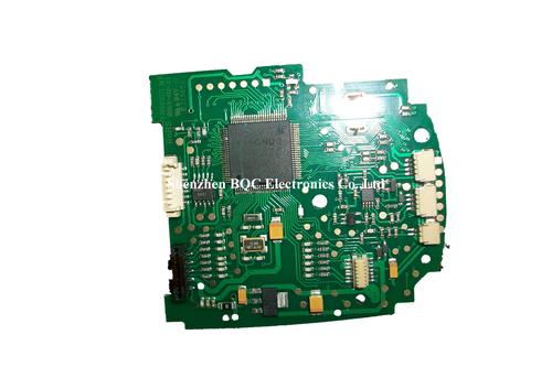
1um=? Mm, 1mil=? The commonly used unit conversion formula for MM circuit board PCB is compiled by Suzhou circuit board sampling manufacturer below. Let's take a look together! For personnel engaged in the PCB industry, it is inevitable to encounter various units of data. Conversion between various units is also frequently needed. It is often necessary to search for conversion values. In order to facilitate the use and learning of PCB practitioners, PCB engineering, PCB electronic engineers, and other personnel. Below are examples of conversion values between various units for your reference. Both Chinese and English abbreviations are indicated. We believe that the unit conversion below is for everyone to keep and learn. Below are examples of conversion values between various units for your reference. Both Chinese and English abbreviations are indicated. We believe that the unit conversion below is for everyone to keep and learn Common units for line width/line spacing/coating th
Previously, the article discussed the packaging and printing methods of aluminum plated films, as well as the principles of ink selection and bonding composite. But this does not mean that only white ink with a high content of resin binder can have sufficient composite adhesion strength. Other factors that affect the adhesion strength of white ink include surface active dispersants and anti sinking, friction resistant wax materials in the ink system, as well as static electricity in the ink itself. The Suzhou circuit board sample manufacturer tells you that once the adhesive is applied to the surface of a white ink film containing surface active dispersants or anti sinking, friction resistant wax additives, the repulsive or almost tensile wax will cause the adhesive layer on the surface of the substrate to form a uniform point like substance, resulting in low-quality packaging printed products with poor composite fastness or low composite strength. Secondly, due to the use of pack
Inquiry Now

