 +86 755 2794 4155
  sales@knownpcb.com
-
Shenzhen KNOWNPCB Technology Co., Ltd.
 +86 755 2794 4155
  sales@knownpcb.com
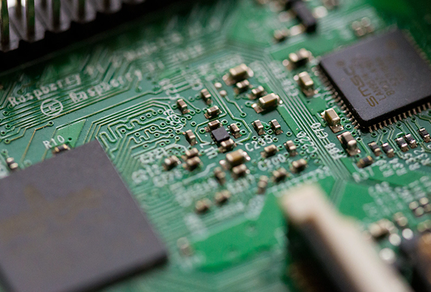
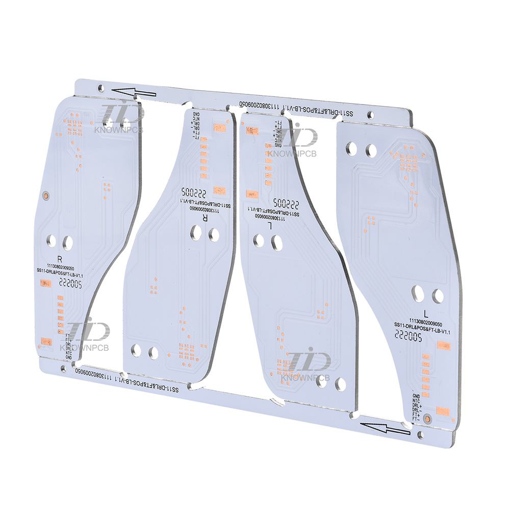
Have you noticed that now more and more of our lighting is using led lighting.What is LED? Compared to the traditional light bulbs, LEDs have lower power consumption, longer lifetime and higher energy efficiency. In the PCB industry,when we say LED PCB, it refers to the pcb used for LED lighting, if you are looking for a suitable LED PCB for your lighting system, this article may bring you something. WHAT ARE LEDS COMPOSED OF?LED is an initial light-emitting diode that produces light when an electric current passes through. LEDs typically have negative and positive electrodes, which generate light in the visible light region.The LEDS are glued to the PCB by soldering process and have electrical connections for lighting.Since light-emitting diodes dissipate a lot of heat when they are in use, when you are designing LED, the metal core is usually the best choice for LED PCB, it is because that it dissipates heat more faster. Among them, the metal material aluminum is the most widely used
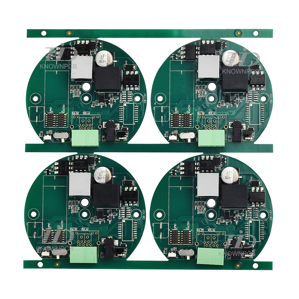
What are some issues to pay attention to in the appearance method of PCB processing? Here are a few points for everyone to have a more comprehensive understanding of some issues related to PCB processing. Understanding these issues clearly is believed that everyone will also gain more knowledge in the field of processing: 1: When adjusting the mold, try to use manual operation instead of manual operation. 2: Start the punching machine and conduct a comprehensive inspection to ensure that all parts, including the clutch, brake, slider, etc., are functioning properly, the operating mechanism is reliable, and there is no continuous punching phenomenon. 3: Prepare several sets of pressure plates and T-head pressure plate screws for use with the mold. The front end of the pressing plate should not touch the straight wall of the lower mold. Sandcloth should be placed between the contact surfaces, and the screws must be tightened. 4: To improve the punching performance of the substrat
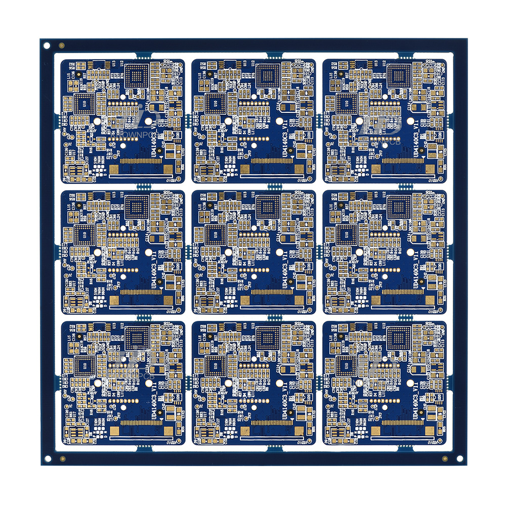
What do we need to know about some passive components in SMT processing? Here you can have a comprehensive understanding of these aspects: 1: Inductor: The ability of a coil to store energy in a magnetic field is called an inductor, and this coil is called an inductor. The main function of inductors is to prevent interference from electromagnetic waves and filter noise in the current. They are widely used, but the technology and scale of chip inductors produced in China are still insufficient, and there is no professional manufacturer of inductors. Resistor: The function of a resistor is to regulate the voltage and current in a circuit, which can be divided into three categories based on material and product packaging. 2: Capacitor: When two conductive substances are separated by a medium and used to store potential static electricity, it is called a capacitor. There are various types of capacitors, which can be divided into more than 30 types based on the materials used. Domest
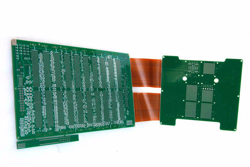
As usual, paying attention to some details can eliminate unwanted situations, such as misprints of solder paste and removal of solidified solder paste from the board. Our goal is to deposit an appropriate amount of solder paste at the desired location. Dirty tools, dry solder paste, and misalignment between the template and the board can all cause unwanted solder paste on the bottom surface of the template or even on the assembly. During the printing process, wipe the template according to a certain pattern between printing cycles. Ensure that the template is located on the solder pad, not on the solder mask layer, to ensure a clean solder paste printing process. Online and real-time solder paste inspection and pre reflow inspection after component installation are both helpful process steps for reducing process defects before welding occurs. For fine-pitch templates, if the thin template cross-section is bent and causes damage between pins, it can cause solder paste to deposit bet
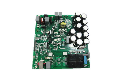
Nowadays, more and more electronic companies are starting to provide personalized PCB board sampling and customization services. There is no fixed range of prices, and prices need to be determined based on the size, quantity, process, special process, delivery time, packaging type, etc. of the circuit board you need to customize. So, how can so many PCB personalized customization companies find a suitable PCB personalized customization company for themselves? This article will explain to you from 8 aspects. Customer Experience A good reputation is the primary factor for us to refer to when choosing personalized customized services for PCB sampling. When selecting a manufacturer for multi-layer PCB board sampling, we can first search for relevant information and information about the manufacturer at the internet level. Manufacturers with their own official website are definitely trustworthy. Only a website is not enough, but it also depends on whether the website has updates on co
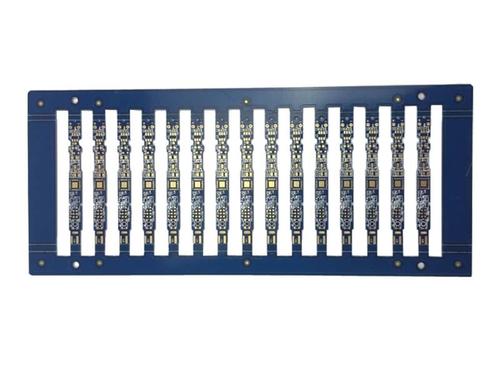
In daily life, the composition of various electronic devices inevitably requires the use of PCB circuit boards. PCB sampling is a provider of electrical connections for electronic components. According to different product design and usage requirements, PCB sampling can also be divided into single-layer boards, double-layer boards, and multi-layer boards. Multilayer boards are currently the most commonly used type of PCB. So what are the application advantages of multi-layer PCB board sampling? Below, the quick technician will organize and introduce for everyone. The application advantages of multi-layer PCB circuit boards: 1. High assembly density, small size, and light weight meet the needs of miniaturization of electronic equipment; 2. Due to the high assembly density, the wiring between various components (including components) is reduced, installation is simple, and reliability is high; 3. Due to the repeatability and consistency of graphics, errors in wiring and assembly a
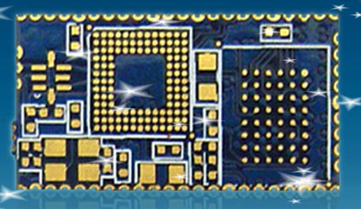
Reflow soldering is a very important process in SMT chip processing, which involves combining the chip components with the solder pads on the circuit board at high temperatures and then cooling them together, greatly affecting the stability of the circuit board. In reflow soldering, some process defects are also prone to occur, and the reasons need to be analyzed and targeted solutions are needed to ensure product quality. Below, the quick technician will mainly organize and introduce the common defects and cause analysis of SMT reflow soldering for everyone. 1、 Tin bead Reason: 1. The silk screen holes are not aligned with the solder pads, and the printing is not accurate, causing solder paste to stain the PCB. 2. Solder paste is exposed too much in an oxidizing environment and absorbs too much water from the air. 3. Heating is inaccurate, too slow and uneven. 4. The heating rate is too fast and the preheating interval is too long. 5. The solder paste dries too quickly. 6.
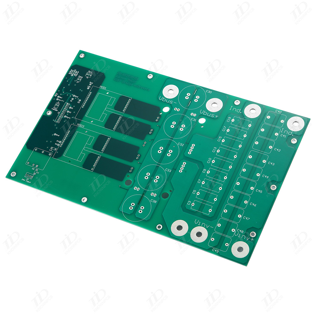
Firstly, the application prospects of microcircuit boards in the field of smartphones are very broad. Nowadays, smartphones have become an essential communication tool in people's lives. The application of micro circuit boards has made smartphones more intelligent and multifunctional. The small size and high integration of microcircuit boards enable smartphones to have stronger computing power and richer functions, such as facial recognition, fingerprint recognition, virtual reality, and so on. Moreover, the rapid development of micro circuit boards has also brought about improvements in the performance and price of smartphones, allowing more people to enjoy the convenience and fun brought by smartphones. Secondly, the application prospects of micro circuit boards in the field of smart homes are also very broad. With the improvement of people's living standards, the requirements for living environment are also increasing. Smart home, as an emerging way of life, is gradually bein
Firstly, one of the difficulties in designing and manufacturing high-frequency high-speed boards is ensuring signal integrity. Due to the transmission characteristics of high-frequency signals, the requirements for signal integrity are very high. Once the signal experiences attenuation, interference, or distortion, it will lead to a decrease in system performance or even malfunction. The key to solving the problem of signal integrity is to choose materials, wiring, and grounding methods reasonably, and conduct strict signal integrity simulation and testing. Secondly, the design and production of high-frequency high-speed boards also face challenges in terms of high-frequency characteristics and electromagnetic compatibility. In the transmission of high-frequency and high-speed signals, electromagnetic wave radiation and interference will become a serious problem. In order to improve electromagnetic compatibility, it is necessary to design and layout devices, pins, and ground wir
Inquiry Now

