 +86 755 2794 4155
  sales@knownpcb.com
-
Shenzhen KNOWNPCB Technology Co., Ltd.
 +86 755 2794 4155
  sales@knownpcb.com
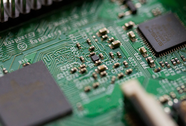
Have you noticed that now more and more of our lighting is using led lighting.What is LED? Compared to the traditional light bulbs, LEDs have lower power consumption, longer lifetime and higher energy efficiency. In the PCB industry,when we say LED PCB, it refers to the pcb used for LED lighting, if you are looking for a suitable LED PCB for your lighting system, this article may bring you something. WHAT ARE LEDS COMPOSED OF?LED is an initial light-emitting diode that produces light when an electric current passes through. LEDs typically have negative and positive electrodes, which generate light in the visible light region.The LEDS are glued to the PCB by soldering process and have electrical connections for lighting.Since light-emitting diodes dissipate a lot of heat when they are in use, when you are designing LED, the metal core is usually the best choice for LED PCB, it is because that it dissipates heat more faster. Among them, the metal material aluminum is the most widely used
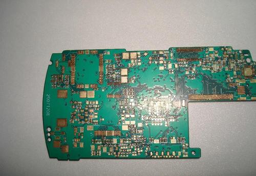
In PCB sampling, nickel is used as a substrate coating for precious and base metals. For some surfaces with heavy load wear, using nickel as the gold substrate coating can greatly improve wear resistance. When used as a barrier layer, nickel can effectively prevent the diffusion between copper and other metals. Next, CITIC Huawei will explain the causes and solutions of PCB nickel plating process faults: 1、 Ma Keng: Ma Keng is the result of organic pollution; If the stirring is poor, bubbles cannot be expelled and pits will form. Large pits usually indicate oil contamination, and wetting agents can be used to reduce their impact. Small pits are called pinholes, which can be caused by poor treatment, metal impurities, low boric acid content, and low plating temperature. Bath maintenance and process control are key, and anti pinhole agents should be used as process stabilizers to supplement. 2、 Roughness and burrs: Roughness indicates that the solution is dirty, which can be correc
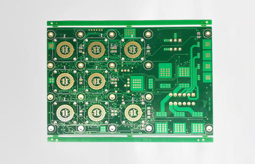
When designing high altitude circuit boards, multi-layer circuit boards are usually used instead of single-layer and double-layer circuit boards. Why is this? Today brings you the reason for using multi-layer boards for high-speed circuit boards! Let's take a look together! Multi layer boards have many characteristics that are not found in single or double layer boards, and it is precisely because of these characteristics that high-speed circuit board designs use multi layer boards instead of other circuit boards. The following is a summary of the characteristics of multi-layer boards! 1. The power supply is very stable; 2. The circuit impedance is significantly reduced; 3. The wiring length is significantly shortened. In addition, from a cost perspective, although the cost of multi-layer circuit boards is higher than that of single-layer circuit boards, the cost difference between multi-layer circuit boards and single-layer circuit boards is not as high as expected when consider
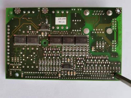
High frequency board refers to a special circuit board with high electromagnetic frequency. Generally speaking, high frequency can be defined as a frequency above 1GHz. The application range of high-frequency circuit boards is very wide, and there are strict requirements in design and manufacturing. So, what are the specific requirements for the production of high-frequency PCB circuit boards? 1. The corner of the transmission line should adopt a 45 ° angle to reduce return loss; 2. The use of high-performance dielectric circuit boards with strictly controlled dielectric constant values according to the number of layers is conducive to effective simulation calculation of the electromagnetic field between insulation materials and adjacent wiring. 3. Produce according to the design specifications for high-precision etching of circuit boards. The total error of the specified line width is+/-0.0007 inches, and overall management of the wiring (wire) geometry and coating surface is c

The size of HDI is limited by the capacity of electronic processing production line equipment, therefore, appropriate HDI size should be considered in product system design. (1) The maximum HDI size that SMT devices can mount comes from the standard size of HDI sheets, most of which are 20 " × 24 ″, i.e. 508mm × 610mm (rail width) (2) The recommended size is a relatively suitable size for each equipment on the SMT production line, which is conducive to maximizing the production efficiency of each equipment and eliminating equipment bottlenecks. (3) For small-sized HDI, it should be designed as a combination to improve the production efficiency of the entire production line. Design Requirements (1) In general, the maximum size of HDI should be limited to 460mm × Within the range of 610mm. (2) The recommended size range is (200-250) mm × (250~350) mm, the aspect ratio should be
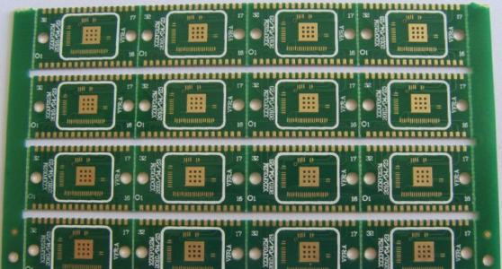
What is HDI (High Density Interconnects) wiring? HDI (High Density Interconnects) wiring refers to the use of the latest design strategies and manufacturing technologies to achieve more dense designs without affecting circuit functionality. In other words, HDI involves the use of multiple wiring layers, smaller wiring, vias, solder pads, and thinner substrates to install complex and usually high-speed circuits within previously impossible footprint areas. With the development of manufacturing technology, HDI wiring has begun to be seen in many designs, such as motherboards, graphics controllers, smartphones, and other space limited devices. If implemented properly, HDI wiring can not only greatly reduce design space, but also reduce EMI issues on PCBs. Reducing costs is an important goal for the company, and HDI cabling can precisely achieve this. It is important to understand that HDI wiring and micro vias are more complex than typical multi-layer wiring strategies. We may have de
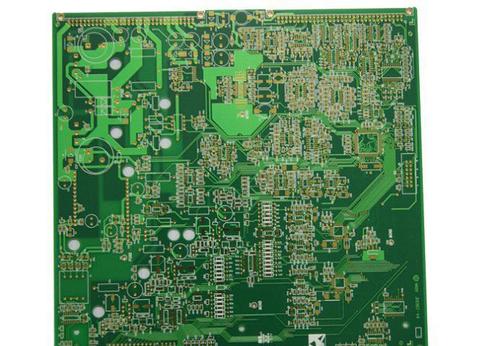
1、 Raw materials The raw materials for PCB sinking gold plates mainly include substrates, electroplating solutions, and chemicals. Among them, the substrate is the main component of the PCB gold plate, and the material and quality of the substrate directly affect the quality of the PCB gold plate. If the material of the substrate is impure or of poor quality, it is easy to cause carbon elements in the PCB gold plate to exceed the standard. 2、 Production process The production process of PCB sinking plates includes multiple processes such as chemical gold plating, electroplated gold plating, and nickel plating. In these links, if the operation is improper or the process is not perfect, it can lead to excessive carbon content in PCB gold plating plates. For example, in the chemical gold plating process, if the temperature, pH value, concentration and other parameters of the plating solution are not suitable, it can lead to excessive carbon content. 3、 Equipment and facilities Th
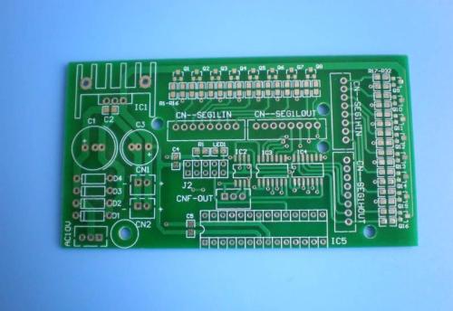
1、 Design phase 1. Preliminary design. The first step in PCB design is to determine the circuit diagram, select components and connect circuits based on the functional requirements of the product. 2. Perform PCB layout. Layout design is the first step after completing circuit design, which requires determining the approximate size and shape of the PCB board, as well as the approximate positions of various components on the board. 3. Wiring design. Designers need to design the connection method and path of the circuit at each layer of the PCB, which is called wiring design. 2、 Material preparation stage 1. Select the substrate. Before starting the production of PCB multilayer boards, it is necessary to choose a suitable substrate, usually fiberglass board. 2. Make copper foil. Copper foil is the most important conductive material in PCB, and thickness selection and production should be based on the design requirements of the PCB. 3. Produce photoresist film. Photoetching film
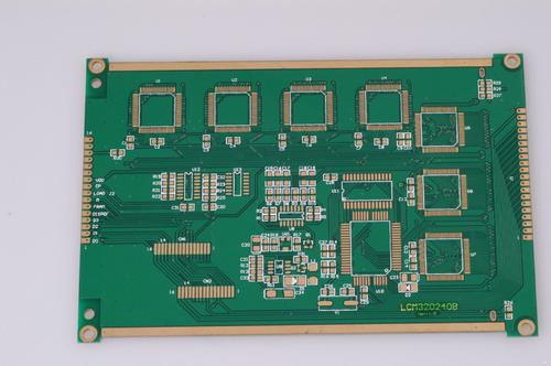
1、 Material selection The production of high-frequency and high-speed printed circuit boards requires the selection of materials with good electrical properties. However, there are many types of materials on the market, and how to choose the appropriate materials has become a challenge. Firstly, it is necessary to consider the dielectric constant and loss factor of the material to ensure the stability and low loss of signal transmission. Secondly, it is also necessary to consider the thermal expansion coefficient and thermal conductivity of the material to avoid size changes and heat accumulation caused by temperature changes. In addition, the machinability and cost of materials also need to be considered. 2、 Design specifications The design of high-frequency and high-speed printed circuit boards needs to comply with certain standards. Firstly, it is necessary to layout the circuit reasonably to reduce the transmission path and interference of the signal. Secondly, it is necessa
Inquiry Now

