 +86 755 2794 4155
  sales@knownpcb.com
-
Shenzhen KNOWNPCB Technology Co., Ltd.
 +86 755 2794 4155
  sales@knownpcb.com
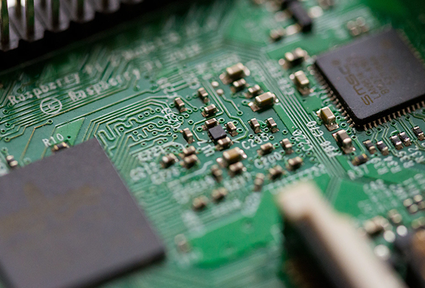
Have you noticed that now more and more of our lighting is using led lighting.What is LED? Compared to the traditional light bulbs, LEDs have lower power consumption, longer lifetime and higher energy efficiency. In the PCB industry,when we say LED PCB, it refers to the pcb used for LED lighting, if you are looking for a suitable LED PCB for your lighting system, this article may bring you something. WHAT ARE LEDS COMPOSED OF?LED is an initial light-emitting diode that produces light when an electric current passes through. LEDs typically have negative and positive electrodes, which generate light in the visible light region.The LEDS are glued to the PCB by soldering process and have electrical connections for lighting.Since light-emitting diodes dissipate a lot of heat when they are in use, when you are designing LED, the metal core is usually the best choice for LED PCB, it is because that it dissipates heat more faster. Among them, the metal material aluminum is the most widely used
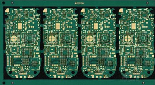
1、 Design considerations When designing multi-layer circuit boards, the following points need to be noted: 1. Determine the number of circuit board layers and interlayer connection methods, reasonably plan the layout of signal and power layers, and avoid signal interference and power noise. 2. Reasonably arrange the size and layout of the circuit board to ensure its manufacturability and assemblability. 3. Choose appropriate line width and spacing to avoid signal crosstalk and current overload. Multilayer circuit board 2、 Material selection considerations When selecting materials for multi-layer circuit boards, the following points need to be noted: 1. Choose high-quality substrate materials, such as FR-4 or high-frequency materials, to ensure the stability and reliability of the circuit board. 2. Choose the appropriate thickness of copper foil, based on current and signal requirements, to avoid overload and signal distortion. 3. Select appropriate interlayer dielectric m
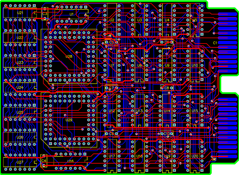
1. Process flow The main process flow of testing and quality inspection includes AOI testing, X-ray testing, antioxidant treatment, and aging treatment, each step of which needs to be strictly executed according to the process. Due to the crucial importance of testing and quality inspection in ensuring product quality and performance, it is necessary to pay more attention to the control of technical points. 2. Technical points In the process of testing and quality inspection, there are several technical points that need special attention: (1) Requirements for AOI testing. In the process of AOI detection, attention should be paid to the hardware and software requirements to ensure the effectiveness and accuracy of the detection. (2) Technical requirements for X-ray detection. In the process of X-ray detection, attention should be paid to the parameters and equipment requirements to ensure the effectiveness and accuracy of the detection. (3) Requirements for antioxidant treatme
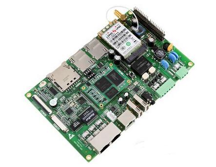
Firstly, we need to consider the specific application scenarios and requirements of PCBs. If a PCB is to be used for high-frequency circuits or high-speed signal transmission, a thinner ink thickness may be more suitable as it can reduce signal transmission loss and reflection. Additionally, if the PCB is to be used in high-temperature environments or circuits with higher power, a thicker ink thickness may be more suitable as it can provide better insulation and heat dissipation performance. Secondly, we also need to consider PCB manufacturing process and cost factors. A thinner ink thickness may require higher manufacturing accuracy and more complex process flow, which may increase manufacturing costs. A thicker ink thickness may be easier to achieve, but it may increase the weight and size of the PCB. Therefore, when selecting ink thickness, it is necessary to comprehensively consider manufacturing process and cost factors. Finally, we also need to consider the reliability and
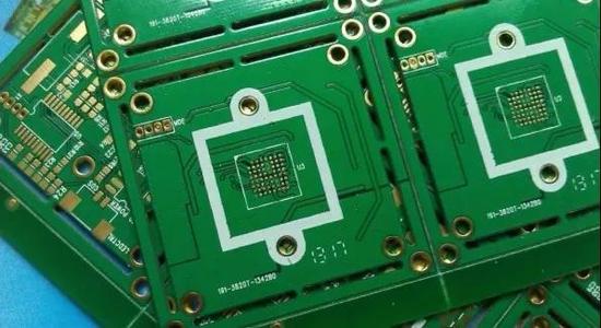
1. Process flow The main process of PCB board production includes graphic design, circuit layout, copper foil coverage, photolithography, etching, drilling, metallization, tin spraying, and organic copper clad board. Each step needs to be strictly executed according to the process. Due to the crucial role played by PCB board production throughout the entire process, great attention should be paid to all production processes. 2. Technical points In the process of PCB board production, there are several technical points that need special attention: (1) Circuit layout. Circuit layout is the foundation of the entire circuit design and one of the key factors determining circuit performance. For high-frequency circuits, attention should be paid to impedance matching and signal interference during the circuit layout process. (2) Photolithography photography. Photolithography refers to the process of amplifying a graphic circuit onto a PCB board through a certain method for comprehens
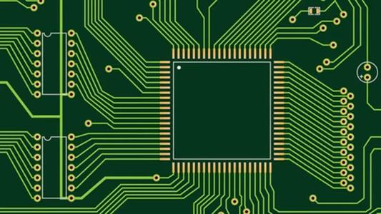
1. Process flow The main process flow of SMT mounting includes printing, mounting, and soldering, and each step needs to be strictly executed according to the process. Due to the significant impact of SMT mounting on circuit stability and reliability, more attention needs to be paid to quality control and technical difficulties in the production process. 2. Technical points In the process of SMT mounting, there are several technical points that need special attention: (1) Selection and use of glue. During the installation process, it is necessary to select appropriate glue to ensure that the components can be pasted onto the PCB board, and also pay attention to the amount of glue used to avoid affecting the heat dissipation of the components. (2) Selection and use of solder paste. During the installation process, it is necessary to select appropriate solder paste to ensure welding quality, while also paying attention to the amount of solder paste used to avoid affecting the we
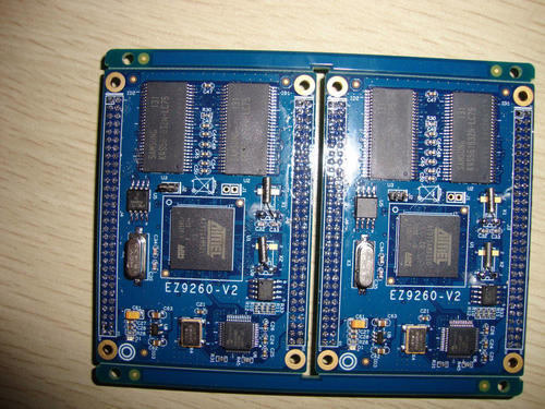
1. Process flow The main process flow of DIP plugins includes insertion, welding, and cutting, each step of which needs to be strictly executed according to the process. Due to the use of DIP plugins in many circuit boards, it is also necessary to pay more attention to quality control and technical difficulties in the production process. 2. Technical points In the process flow of DIP plugins, there are several technical points that need special attention: (1) The depth of pin insertion. During the insertion process, it is necessary to pay attention to the depth of insertion to ensure the stability of the plugin and the reliability of the connection. (2) Control of welding temperature and time. During the welding process, it is necessary to strictly control the welding temperature and time to ensure the quality and consistency of the welding. (3) Key technical points for cutting. During the cutting process, it is necessary to pay attention to the cutting angle and force to ens

Usually, when the board is relatively dense, we use vias of the size of 8/16 ± 2mil (8/14, 8/16, 8/18 can be used). When the board is relatively open, we can choose vias of the size of 12/24 ± 2mil (12/22, 12/24, 12/26 can be used). If the device density of the board is between the two, vias of the size of 10/20 ± 2mil (10/18, 10/20, 10/22 can be used). From the perspective of economic benefits, the larger the through-hole, the lower the cost. Therefore, if we want to control the cost of the board, we should try to set the through-hole as large as possible while meeting our design requirements. Of course, in HDI boards, we usually need to use blind buried holes. Usually, the size range of our blind holes can be set to 4/10 ± 2, which is usually enough to be punched on the solder pad. However, it should be noted that they should not be punched on the center of the solder pad, usually on the edge of the solder pad, which will improve the process treatment. So, is it better for our
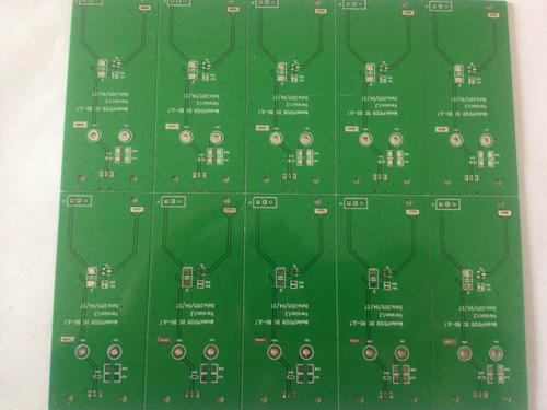
As is well known, impedance control is the most fundamental principle in our high-speed design. At present, conventional board factories control the impedance to an error of 10%, and many friends may have questions, why is it 10%? In theory, the smaller the error, the better, so why not further increase the conventional control capability to 8%, or even 5%? Ideals may be beautiful, but reality is inevitably cruel. There are many factors that affect the impedance of PCB wiring, mainly including the width and thickness of the copper wire, the dielectric constant of the medium, the thickness of the medium, and the thickness of the solder mask. Therefore, in order to minimize the impedance error, it is necessary to control the errors of various factors mentioned above very well during the PCB processing process, in order to ultimately achieve a small impedance error. But looking at the PCB processing process step by step, you will find that almost every process produces errors in the
Inquiry Now

