 +86 755 2794 4155
  sales@knownpcb.com
-
Shenzhen KNOWNPCB Technology Co., Ltd.
 +86 755 2794 4155
  sales@knownpcb.com
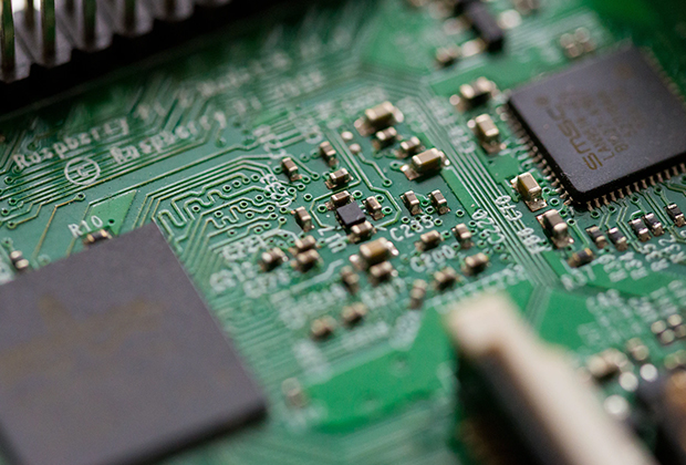
Have you noticed that now more and more of our lighting is using led lighting.What is LED? Compared to the traditional light bulbs, LEDs have lower power consumption, longer lifetime and higher energy efficiency. In the PCB industry,when we say LED PCB, it refers to the pcb used for LED lighting, if you are looking for a suitable LED PCB for your lighting system, this article may bring you something. WHAT ARE LEDS COMPOSED OF?LED is an initial light-emitting diode that produces light when an electric current passes through. LEDs typically have negative and positive electrodes, which generate light in the visible light region.The LEDS are glued to the PCB by soldering process and have electrical connections for lighting.Since light-emitting diodes dissipate a lot of heat when they are in use, when you are designing LED, the metal core is usually the best choice for LED PCB, it is because that it dissipates heat more faster. Among them, the metal material aluminum is the most widely used
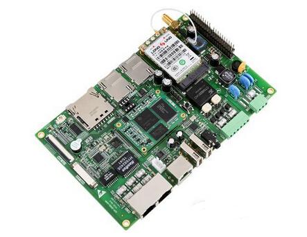
On printed circuit boards, all electrical connections of components are made through solder pads. According to different components and welding processes, pads can be divided into two types: non through hole pads and through hole pads. Non through hole pads are mainly used for welding surface mount components, while through hole pads are mainly used for welding pin type components. So, what are the shapes of solder pads? Next, please come with the editor to understand: 1. Circular pad In PCB sampling, circular pads are the most commonly used type of pad. For through-hole pads, the main dimensions of circular pads are the through-hole size and pad size, and the pad size is generally twice the through-hole size. Non through-hole circular pads are mainly used for testing pads, positioning pads, and reference pads, and their main dimensions are pad sizes. 2. Rectangular pad There are two types of rectangular pads: square and rectangular. The square pad is mainly used to identify
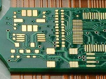
Rigid circuit boards include phenolic paper laminates, epoxy paper laminates, polyester glass felt laminates, and epoxy glass cloth laminates. Flexible printed circuit boards are also known as flexible printed circuit boards or FPCs. Flexible circuit board, also known as FPC or soft board, is a type of printed circuit board that uses polyimide or polyester film as the substrate, has high reliability and flexibility. So, what are the characteristics of flexible circuit boards and rigid circuit boards? 1、 Characteristics of rigid circuit boards: 1. High density. With the improvement of circuit integration and the advancement of mounting technology, high-density printed circuit board technology has become very mature. 2. High reliability. Through a series of inspections, tests, and aging tests, it can be ensured that the PCB works reliably for a long time. 3. Designability. For various performance requirements of PCBs (electrical, physical, chemical, mechanical, etc.), circuit b
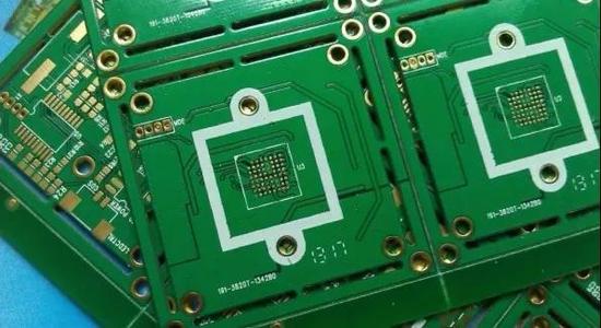
Nowadays, the use of PCB multilayer circuit boards on the market has become a popular trend, and in the development of the industry, the ability of many PCB manufacturers to develop and produce PCB multilayer circuit boards has become increasingly prominent. So, what are the requirements for PCB multi-layer circuit board sampling? Below, the editor will analyze for everyone: 1. Requirements for clean appearance. When making samples for PCB multilayer circuit boards, it is necessary to have a flat appearance of the template, no burrs on the edges and corners, and no blistering or delamination between the wires and solder mask. Only in this way can the PCB multi-layer circuit board ensure better welding effect and also ensure that the PCB multi-layer circuit board produced by the PCB manufacturer meets the appearance requirements of actual use. 2. Reasonable process requirements. Before sampling, it is also necessary to study whether the process of PCB multilayer circuit boards is
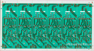
Many customers often confuse rigid flex bonding boards and IC carrier boards. Let a professional PCB factory provide you with a detailed explanation of rigid flex bonding boards and IC carrier boards? 1. What is a rigid flexure composite plate? Rigid flexible combination board refers to the combination of soft and hard boards, which combines a thin layer of flexible and rigid bottom layers, and then presses them into a single component to form a circuit board. It has the characteristics of being flexible and foldable. Due to the mixed use of multiple materials and multiple production steps, the processing time of rigid flexible composite plates is longer and the production cost is higher. In the PCB sampling of electronic consumer products, the use of rigid flexible combination boards not only maximizes space usage and minimizes weight, but also greatly improves reliability, thereby eliminating many demands for welded joints and fragile wiring that are prone to connection proble

Medical PCB board is the supporting part of circuit components and equipment in electronic products. Even if the circuit schematic design is correct or the printed circuit board design is inappropriate, it can have a negative impact on the reliability of electronic products. So design according to certain principles. 1. The principles that should be followed in the layout design of medical PCB boards: Firstly, consider the size of the medical PCB board. When the PCB size is too large, the printing line will be long, the impedance will increase, the noise resistance will decrease, and the cost will increase; If the PCB size is too small, the heat dissipation effect will be poor, and adjacent circuits will be easily disturbed. After determining the size of the printed circuit board, it is also necessary to determine the location of special components. Then, according to the functional units of the circuit, arrange all components of the circuit. When determining the location of speci

So, how to store the half hole PCB board of the module? Circuit boards are not better than other products and cannot come into contact with gases and water. Cannot damage the module half hole PCB vacuum pump. When loading, place a layer of foam pad beside the small box. Bubble pads have better water absorption ability and are very effective in waterproofing. Naturally, waterproof beads are also essential. Then classify and label the sewage. After opening the packaging, the small box must be separated from the wall, stored off the ground in a dry and cool place, and protected from sunlight. Module half hole PCB boards that have undergone metal surface treatment (such as gold immersion, electroplating, tin spray painting, gold plating, etc.) can usually be stored for 6 months, while module half hole PCB boards that have undergone metal surface treatment (such as silver immersion) can usually be stored for 6 months., Tin, OSP, etc. can usually be stored for 3 months. For module half
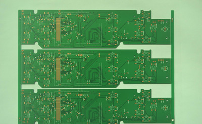
Module half hole PCB board. A double-layer PCB circuit board is a type of PCB circuit board formed by bonding a replaced conductive pattern layer and an insulating layer material layer. The number of stacked layers of the conductivity pattern is above three, and the interconnection of fixed layer electrical equipment is completed based on metallized holes. If one double-sided board is used as the inner layer, two single-sided aluminum substrates are used as the outer layer, or two double-sided boards are used as the inner layer, and two single-sided aluminum substrates are used as the outer layer, and the raw materials are bonded together according to the system and insulation layer, and the conductivity pattern is interconnected according to the design plan, it becomes a four or six layer PCB circuit board, also known as a double-layer PCB circuit board. A double panel is a material layer in the middle, and both sides are wiring layers. The double-layer module half hole PCB board
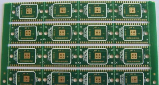
Another reason for this problem is that the composition of the solder wire used throughout the production, processing, and manufacturing process changes, resulting in excessive residue and the need to add pure tin or replace the solder wire. Spot printed laminated glass undergoes changes in the physical state of chemical fiber layers, such as separation between layers. But this type of situation is not due to poor spot welding. The reason is that the base steel plate is too hot, so it is necessary to reduce the heating and soldering wire temperature or increase the driving speed of the base steel plate. In general, the solder wire of the module half hole PCB board appears dark gray, but sometimes there are orange spot welds. The key reason for this problem is that the temperature is too high, and only lowering the temperature of the tin furnace is sufficient. Due to the structure of the PCB itself, it is very easy to cause harm to the module's half hole PCB board when exposed to
Inquiry Now

