 +86 755 2794 4155
  sales@knownpcb.com
-
Shenzhen KNOWNPCB Technology Co., Ltd.
 +86 755 2794 4155
  sales@knownpcb.com
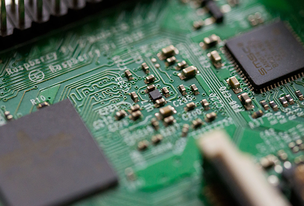
Have you noticed that now more and more of our lighting is using led lighting.What is LED? Compared to the traditional light bulbs, LEDs have lower power consumption, longer lifetime and higher energy efficiency. In the PCB industry,when we say LED PCB, it refers to the pcb used for LED lighting, if you are looking for a suitable LED PCB for your lighting system, this article may bring you something. WHAT ARE LEDS COMPOSED OF?LED is an initial light-emitting diode that produces light when an electric current passes through. LEDs typically have negative and positive electrodes, which generate light in the visible light region.The LEDS are glued to the PCB by soldering process and have electrical connections for lighting.Since light-emitting diodes dissipate a lot of heat when they are in use, when you are designing LED, the metal core is usually the best choice for LED PCB, it is because that it dissipates heat more faster. Among them, the metal material aluminum is the most widely used
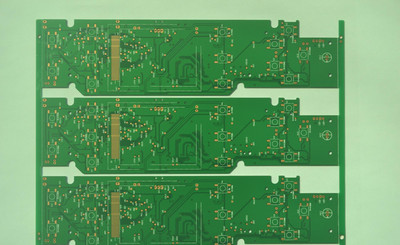
1. Why do I need to plug holes when BGA is in resistance welding? What are the acceptance criteria? Answer: Firstly, the solder plug hole is to protect the service life of the through hole. The hole diameter required for the BGA position plug is generally relatively small, ranging from 0.2 to 0.35mm. During the subsequent processing, some of the medicine in the hole is not easy to dry or evaporate, and it is easy to leave residue. If the solder plug hole is not plugged or not full during the solder plug, there will be residual foreign objects or solder beads in the subsequent processing such as tin spraying and gold deposition, which will be heated when the customer installs the component for high-temperature welding, Foreign objects or tin beads inside the hole will flow out and adhere to the component, causing defects in the performance of the component, such as open circuit or short circuit. BGA is located in the solder plug hole A. Be sure to plug it fully. B. There should be
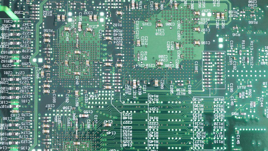
After several waves of upward momentum, PCB factories have already reached their limits in terms of affordability. It is understood that in the past six months, the average price of CCL materials has increased by about 20-30%. Therefore, most PCB manufacturers, especially traditional hard board manufacturers, can no longer withstand the pressure and have started price negotiations with customers, hoping that customers can understand the pressure from PCB factories and help absorb some costs. The end customers, ODM and OEM factories that are in contact with PCB factories have seen a real shortage of materials, and the pressure to rush out far outweighs the cost pressure. Recently, their attitudes have indeed softened. It is widely believed that although the magnitude of the price increase cannot be determined, the cost transfer negotiations among PCB factories are expected to achieve certain results. Even if the price increase is only 5-10%, it can be considered as a small supplemen

The main purpose of PCB baking is to remove moisture and moisture, removing moisture inside or absorbed from the outside of the PCB, as some PCBs themselves use materials that easily form water molecules. In addition, after PCB production and placement for a period of time, there is also a chance to absorb moisture from the environment, and water is one of the main culprits causing PCB explosion or delamination. Because when the PCB is placed in an environment with a temperature exceeding 100 ℃, such as a reflow furnace, wave soldering furnace, hot air leveling, or manual welding process, water will become water vapor and quickly expand its volume. The faster the heating speed on the PCB, the faster the expansion of water vapor; The higher the temperature, the larger the volume of water vapor; When water vapor cannot escape from the PCB in a timely manner, there is a good chance of expanding the PCB. Especially the Z direction of a PCB is the most fragile, sometimes it may brea
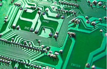
At present, the formation process of refined circuits includes laser imaging (pattern transfer) and pattern etching forming. Laser direct imaging (LDI) technology is the process of obtaining refined circuit patterns directly by laser scanning on the surface of copper clad plates coated with photoresist. Laser imaging technology greatly simplifies the process flow and has become the mainstream technology in HDI PCB plate making. The application of semi additive method (SAP) and improved semi additive method (mSAP), namely graphic etching method, is increasing nowadays. This technology process can also achieve conductive circuits with a line width of 5um. How to improve electroplating uniformity and deep hole plating ability in PCB manufacturing, and improve the reliability of the board. This depends on the continuous improvement of the electroplating process, starting from various aspects such as the proportion of electroplating solution, equipment allocation, and operating proce
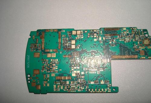
With the development of technology, some high-tech devices are becoming increasingly miniaturized and precise, which puts higher demands on the HDI boards they use. The line width/spacing of HDI circuit boards for some devices has evolved from early 0.13 mm (5 mils) to 0.075 mm (3 mils) and has become a mainstream standard. As a leading enterprise in the HDI fast board industry, Shenzhen Benqiang Circuit Co., Ltd. has achieved a production process of 38 μ M (1.5 mil) is approaching the limit of the industry. The increasingly high requirements for line width/distance have brought the most direct challenge to graphic imaging in the PCB manufacturing process. So how are the copper wires on these precision boards processed and formed? The important feature of HDI circuit boards is the presence of micro through holes (aperture ≤ 0.10 mm), all of which belong to buried blind hole structures. The buried blind holes on HDI boards are currently mainly processed by laser, but there are a
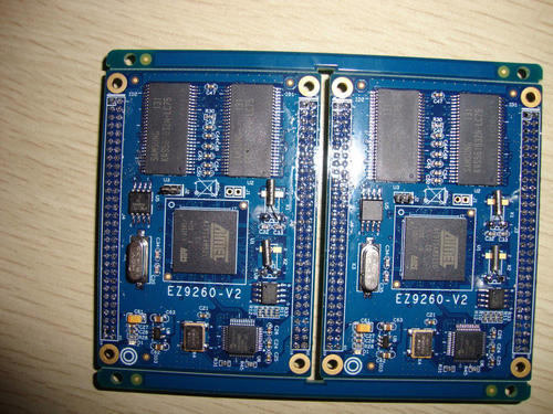
PCB circuit board impedance refers to the parameters of resistance and reactance, which hinder AC power. In the production of PCB circuit boards, impedance processing is essential. The reasons are as follows: 1. PCB circuits (bottom of the board) should consider the installation of electronic components by plugging, and after plugging, issues such as conductivity and signal transmission performance should be considered. Therefore, it is required that the impedance should be as low as possible, and the resistivity should be less than 1&TIMes per square centimeter; Below 10-6. 2. During the production process of PCB circuit boards, they need to go through processes such as copper deposition, electroplating tin (or chemical plating, or thermal spraying tin), and connector soldering. The materials used in these processes must ensure a low resistivity to ensure that the overall impedance of the circuit board meets product quality requirements and can operate normally. 3. The tin plat
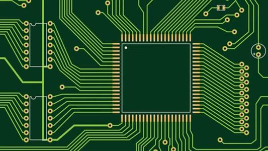
For the electronics industry, according to industry surveys, the most fatal weaknesses of chemical tin plating are its susceptibility to discoloration (i.e. oxidation or deliquescence), poor solderability leading to difficulty in soldering, high impedance leading to poor conductivity or unstable overall board performance, and susceptibility to tin growth, which can lead to short circuits in PCB circuits and even burning or ignition events. It is reported that Kunming University of Technology in the early 1990s was the first to study chemical tin plating in China, followed by Guangzhou Tongqian Chemical (Enterprise) in the late 1990s. It has been recognized in the industry for the past 10 years that these two institutions are doing the best. Among them, according to our contact screening investigations, experimental observations, and long-term endurance tests of numerous enterprises, it has been confirmed that the tin coating of Tongqian Chemical is a pure tin layer with low resist
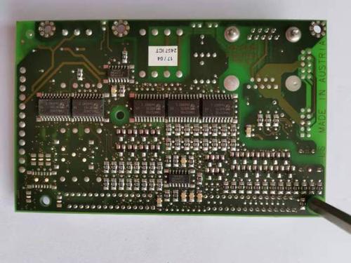
(1) Characteristic impedance In electronic information products such as computers and wireless communication, the energy transmitted in the circuit of a PCB is a square wave signal (pulse) composed of voltage and time, and the resistance it encounters is called characteristic impedance. (2) Differential impedance Two identical signal waveforms with opposite input polarity at the driving end are transmitted by two differential lines, and these two differential signals are subtracted at the receiving end. The differential impedance is the impedance Zdiff between two lines. (3) Odd mode impedance The impedance of one line to ground in the two lines is consistent. (4) Even mode impedance The impedance Zcom of two identical signal waveforms with the same input polarity at the driving end when connecting the two wires together. (5) Common mode impedance The impedance Zoe of one line to ground in the two lines is consistent, usually greater than the odd mode impedance.
Inquiry Now

