 +86 755 2794 4155
  sales@knownpcb.com
-
Shenzhen KNOWNPCB Technology Co., Ltd.
 +86 755 2794 4155
  sales@knownpcb.com
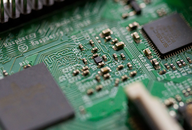
Have you noticed that now more and more of our lighting is using led lighting.What is LED? Compared to the traditional light bulbs, LEDs have lower power consumption, longer lifetime and higher energy efficiency. In the PCB industry,when we say LED PCB, it refers to the pcb used for LED lighting, if you are looking for a suitable LED PCB for your lighting system, this article may bring you something. WHAT ARE LEDS COMPOSED OF?LED is an initial light-emitting diode that produces light when an electric current passes through. LEDs typically have negative and positive electrodes, which generate light in the visible light region.The LEDS are glued to the PCB by soldering process and have electrical connections for lighting.Since light-emitting diodes dissipate a lot of heat when they are in use, when you are designing LED, the metal core is usually the best choice for LED PCB, it is because that it dissipates heat more faster. Among them, the metal material aluminum is the most widely used
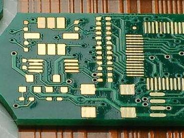
HDI board (High Density Interconnector), also known as high-density interconnect board, is a circuit board that uses micro blind buried hole technology and has a relatively high line distribution density. The HDI board has both inner and outer circuits, which are connected internally by drilling and metallization processes. HDI boards are generally manufactured using the stacking method, and the more times they are stacked, the higher the technical level of the board. Ordinary HDI boards are basically stacked once, while higher-order HDI uses two or more layers of technology, as well as advanced PCB technologies such as hole stacking, electroplating filling, and laser direct drilling. When the density of PCBs increases beyond eight layers, manufacturing with HDI will result in lower costs compared to traditional complex pressing processes. HDI boards are conducive to the use of advanced assembly technology, and their electrical performance and signal accuracy are higher than trad
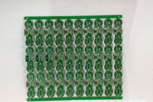
Answer: (1) Solder resist oil is generally composed of a mixture of the main agent, curing agent, and diluent of the ink. During the mixing and stirring of the ink, there will be some air left in the liquid. When the ink is squeezed by a scraper or screen, it flows onto the board surface. In a short period of time, when it encounters strong light or equivalent temperature, the gas inside the ink will flow rapidly with the accelerated flow of the ink, and evaporate outward. (2) The spacing between the lines is too narrow, and the lines are too high. During screen printing, the solder mask ink cannot print onto the substrate, resulting in the presence of air or moisture between the solder mask ink and the substrate. During curing and exposure, the gas expands and causes bubbles due to heat. (3) Single lines are mainly caused by high lines. When the scraper contacts the line, the angle between the scraper and the line increases, making the solder mask ink unable to print to the bottom
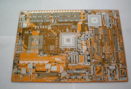
The signal integrity problem is not caused by a single factor, but by multiple factors in board level design. The main signal integrity problems include reflection, ringing, ground bounce, crosstalk, etc. The following mainly introduces the solutions to crosstalk and reflection. Cross talk refers to the unwanted voltage noise interference caused by electromagnetic coupling on adjacent transmission lines when a signal propagates on the transmission line. Excessive crosstalk may cause false triggering of the circuit, resulting in the system not functioning properly. Due to the inverse ratio between crosstalk and line spacing, it is proportional to the parallel length of the lines. Crosstalk varies with the load of the circuit, and for the same topology and wiring situation, the larger the load, the greater the crosstalk. Crosstalk is directly proportional to the signal frequency. In digital circuits, the edge change of the signal has the greatest impact on crosstalk. The faster the
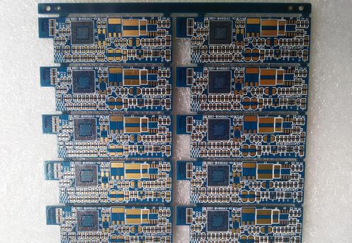
Signal integrity refers to the ability of a signal to respond with the correct timing and voltage in a circuit. It is a state in which the signal is undamaged and represents the quality of the signal on the signal line. 1 Delay Delay refers to the limited speed at which a signal is transmitted on the wires of a PCB board, and there is a transmission delay between the signal being sent from the sending end to the receiving end. The delay of the signal will have an impact on the timing of the system, and the transmission delay mainly depends on the length of the wire and the dielectric constant of the surrounding medium. In high-speed digital systems, the length of signal transmission lines is the most direct factor affecting the phase difference of clock pulses. Clock pulse phase difference refers to the asynchronous arrival of two clock signals at the receiving end. The phase difference of clock pulses reduces the predictability of signal arrival. If the phase difference of clo
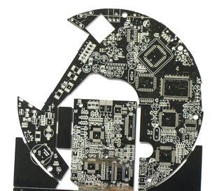
As the speed of integrated circuit output switches increases and the density of PCB boards increases, Signal Integrity has become one of the essential issues in high-speed digital PCB design. Factors such as the parameters of components and PCB boards, the layout of components on the PCB board, and the layout of high-speed signal lines can all cause signal integrity issues. For PCB layout, signal integrity requires providing a circuit board layout that does not affect signal timing or voltage, while for circuit wiring, signal integrity requires providing termination components, layout strategies, and wiring information. High signal speed, incorrect layout of termination components, or incorrect wiring of high-speed signals on a PCB can all cause signal integrity issues, which may result in incorrect system output, abnormal circuit operation, or even complete failure. How to fully consider signal integrity factors and take effective control measures in the PCB design process has b
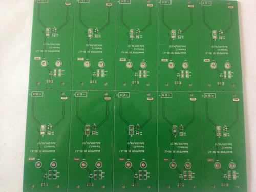
Answer: 1. The circuit board surface includes a foil coated substrate and a pre copper plated substrate after hole metallization. To ensure a firm adhesion between the dry film and the substrate surface, it is required that the substrate surface be free of oxide layers, oil stains, fingerprints, and other dirt, drilling burrs, and rough coatings. To increase the contact area between the dry film and the substrate surface, it is also required that the substrate have a micro rough surface. To meet the above two requirements, the substrate must be carefully treated before applying the film. The treatment methods can be summarized into two categories: mechanical cleaning and chemical cleaning. 2. The same principle applies to resistance welding. Before resistance welding, grinding the plate is to remove some oxidation layers, oil stains, fingerprints, and other dirt from the plate surface. In order to increase the contact area between the resistance welding ink and the plate surface and
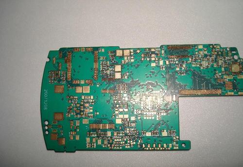
With the continuous enhancement of mobile terminal functions and the continuous development of thinness and lightness, the design of HDI boards is more towards third-order or even any layer HDI boards. Apple has adopted any layer of HDI for the first time in iPhone 4 and iPad 2, significantly improving the product's lightness and thinness. Subsequently, the Android camp quickly followed suit, and any layer of HDI became the standard motherboard for current mid to high-end smartphones. According to statistics, changing from first-order HDI to any layer HDI can reduce the volume by about 40%. It is expected that any layer of HDI will be applied in an increasing number of high-end smartphones and tablets in the future. At present, the adoption rate of third-order HDI and any layer HDI for smartphones is about 30%, while the adoption rate for tablets is even higher at over 80%. We believe that mobile terminals represented by smartphones will continue to drive the development of HDI boa
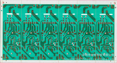
In addition to mobile terminals, high-end servers will also drive up the overall demand level for HDI. Currently, PCBs with layers below 8 are mainly used for household appliances, PCs, desktop computers, etc., while high-end applications such as high-performance multi-channel servers and aerospace require PCBs with layers above 10. Taking servers as an example, on single or dual channel servers, PCB boards are generally between 4-8 layers, while high-end servers such as 4-way and 8-way require 16 layers or more on the motherboard and 20 layers or more on the backplane. Therefore, HDI boards are more commonly used. The development of the domestic cloud computing market and the rapid expansion of mobile internet such as mobile payments, OTO applications, and social networks have driven the steady growth of the Chinese server market, becoming the main driving force for global shipment growth, and the growth rate is constantly increasing. In 2015, the sales revenue was 49.82 billion
Inquiry Now

