 +86 755 2794 4155
  sales@knownpcb.com
-
Shenzhen KNOWNPCB Technology Co., Ltd.
 +86 755 2794 4155
  sales@knownpcb.com
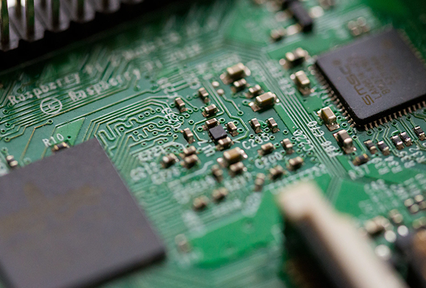
Have you noticed that now more and more of our lighting is using led lighting.What is LED? Compared to the traditional light bulbs, LEDs have lower power consumption, longer lifetime and higher energy efficiency. In the PCB industry,when we say LED PCB, it refers to the pcb used for LED lighting, if you are looking for a suitable LED PCB for your lighting system, this article may bring you something. WHAT ARE LEDS COMPOSED OF?LED is an initial light-emitting diode that produces light when an electric current passes through. LEDs typically have negative and positive electrodes, which generate light in the visible light region.The LEDS are glued to the PCB by soldering process and have electrical connections for lighting.Since light-emitting diodes dissipate a lot of heat when they are in use, when you are designing LED, the metal core is usually the best choice for LED PCB, it is because that it dissipates heat more faster. Among them, the metal material aluminum is the most widely used
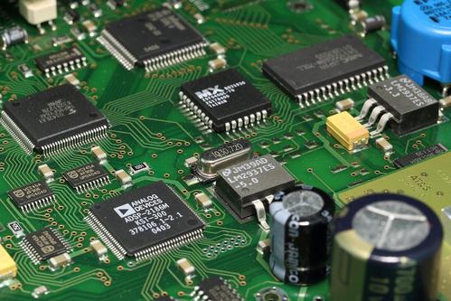
The working environment of circuit boards can be subject to different external disturbances, which may come from power sources, spatial electromagnetic fields, and ground wires. So, what are the measures for suppressing interference on circuit boards? 1. Filter: A filter is a network composed of resistors, inductors, and capacitors with lumped or distributed parameters, used to separate noise superimposed on useful signals. The filter has a good effect on suppressing transient noise of inductive loads, and connecting the power input to the filter can reduce electromagnetic interference from the power grid. 2. Shielding: Shielding refers to the absorption or reflection of external electromagnetic interference by various shielded objects to prevent noise intrusion; Alternatively, limit the electromagnetic energy radiated inside the device to prevent interference with other devices. 3. Reasonable wiring: The type of wire, the thickness of wire diameter, the way of wiring, the dist
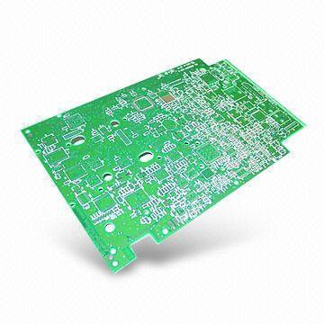
Many customers often overlook many key points when seeking circuit board manufacturers for circuit board sampling, resulting in unsatisfactory circuit board samples and unnecessary losses. So, what are the key considerations for circuit board sampling? 1. Quality The first thing to note is the quality of the circuit board. The selection of boards, the use of ink, production equipment, and the rigor of staff all affect the final quality of circuit boards. 2. Delivery date Customers have all had this experience: the circuit board manufacturer promised delayed sample delivery and found various reasons. Circuit board manufacturers can greatly improve production efficiency and ensure delivery speed only by implementing strict process management during the production process. 3. Price The customer is also very concerned about the price of circuit board samples. The factors that affect the price are the number of layers, thickness, material, order quantity, surface treatment process
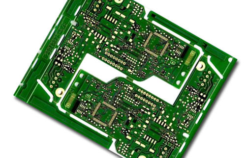
Double panel is a type of circuit board product that customers make a lot. So, how to design a regular double-sided circuit board? Let Shenzhen Circuit Board Factory provide you with a detailed explanation: 1. The common design is that the surface layer is power supply+signal, and the bottom layer is ground+signal. The power supply and ground can adopt a cross bus structure or a large area of copper coating, depending on the actual wiring space. 2. Another good design idea is to implement each layer according to the design requirements of a single panel, and then further adjust and optimize it, such as thickening the power supply/ground wire, and laying copper on large areas of spare parts. 3. When manually wiring, it is necessary to follow some general design guidelines: try to use a ground plane as the current circuit, and separate the analog ground plane from the digital ground plane. If the ground plane is separated by signal wiring, in order to reduce interference with the
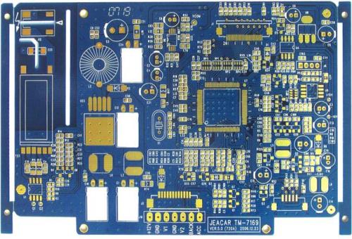
Circuit boards have many "layers", and many beginners are easily confused by various layers of circuit boards when learning circuit board design. Below, let the engineer summarize the definitions of various layers in circuit board design for you to help you better understand and master. 1. Mechanical layer Usually used to place indicative information about circuit boards and assembly methods, such as circuit board dimensions, size markings, data, assembly instructions, and other information. 2. Occlusive layer Draw a closed area on this layer as the effective area for wiring, which cannot be automatically arranged and routed. 3. Silk screen layer The silk screen layer is a text layer that belongs to the top layer of a circuit board and is typically used to mark the projected contour of components, their labels, nominal values or models, and various annotation characters. 4. Welding layer The solder entry layer is the green part of the printed circuit board. After mapping th
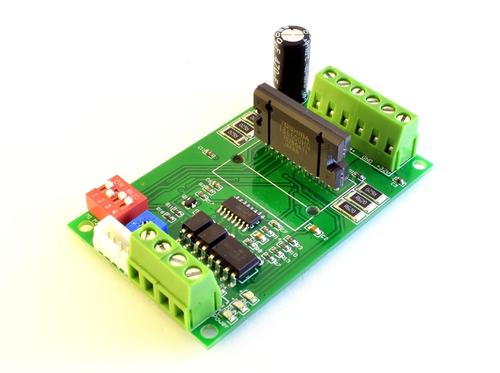
During the design and production process of circuit boards, various problems are always encountered, such as circuit board short circuits, circuit board open circuits, and circuit board solder joints turning golden. Next, let the engineer explain the common problems and cause analysis of circuit board sampling for you in detail. 1. Circuit board short circuit This is one of the common faults in circuit board production, and there are many reasons for this problem: 1) The biggest cause of circuit board short circuits is improper design of welding pads; At this point, the circular welding pad can be changed to an oval shape, increasing the distance between points. 2) Improper design of the direction of circuit board components can also cause short circuits. 3) Automatic plug-in bending foot. It can also cause a short circuit on the circuit board. 4) Other reasons, such as large substrate holes, low tin furnace temperature, poor solderability of the board surface, failure of sol
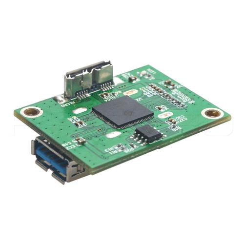
Circuit board design is a crucial step before circuit board production. So, for beginners, what issues do circuit board design need to understand? Let the engineer share with you: 1. Create packages that are not in the package library. Build using the encapsulation model editor to ensure that the encapsulation model used for the encapsulation library is complete and to ensure the smooth progress of circuit board design. 2. Set circuit board design parameters. According to the needs of circuit system design, set the number of layers, size, color, etc. of the circuit board. 3. Load the network table. Load the web table generated from the schematic diagram and automatically load the component encapsulation model into the circuit board design window. 4. Layout. Combining automatic and manual layout, placing the component packaging model in an appropriate position within the planning range of the circuit board ensures a neat and aesthetically pleasing component layout, which is bene
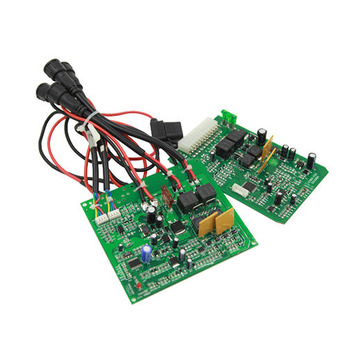
Circuit boards are prone to solder back issues during production, resulting in bending and warping of the board, which affects the product qualification rate. So, how to reduce the risk of bending and deformation in circuit board production? 1. The effect of reducing temperature on the stress of circuit boards. Due to temperature being the main source of stress on circuit boards, as long as the temperature of the reflow furnace is reduced or the production heating speed of the circuit board in the welding furnace is slowed down, the bending and warping of the board can be greatly reduced. 2. The use of boards with higher Tg can increase their ability to withstand stress deformation, but the production cost of circuit boards is also relatively high. 3. Increase the thickness of the circuit board. Many electronic products have circuit board thicknesses of 1.0mm, 0.8mm, or 0.6mm for lighter purposes. It is recommended that if there are no requirements, the circuit board should be 1
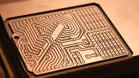
In recent years, with the development of circuit board welding technology, reflow welding technology has become a trend. Below, let Shenzhen circuit board manufacturers explain in detail: What are the three main factors that constitute welding defects in circuit boards? 1. The solderability of circuit board holes affects welding quality The poor solderability of circuit board holes will result in solder defects, affecting the parameters of components in the circuit, causing unstable conduction of multi-layer board components and inner wires, and leading to the failure of the entire circuit function. 2. Welding defects caused by warping of circuit boards The circuit board and components produce warping during the welding process, resulting in defects such as solder joints and short circuits due to stress deformation. Warping is often caused by uneven temperature distribution between the upper and lower parts of a circuit board. In addition, for large-sized circuit boards, they m
Inquiry Now

