 +86 755 2794 4155
  sales@knownpcb.com
-
Shenzhen KNOWNPCB Technology Co., Ltd.
 +86 755 2794 4155
  sales@knownpcb.com
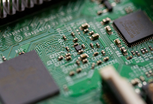
Have you noticed that now more and more of our lighting is using led lighting.What is LED? Compared to the traditional light bulbs, LEDs have lower power consumption, longer lifetime and higher energy efficiency. In the PCB industry,when we say LED PCB, it refers to the pcb used for LED lighting, if you are looking for a suitable LED PCB for your lighting system, this article may bring you something. WHAT ARE LEDS COMPOSED OF?LED is an initial light-emitting diode that produces light when an electric current passes through. LEDs typically have negative and positive electrodes, which generate light in the visible light region.The LEDS are glued to the PCB by soldering process and have electrical connections for lighting.Since light-emitting diodes dissipate a lot of heat when they are in use, when you are designing LED, the metal core is usually the best choice for LED PCB, it is because that it dissipates heat more faster. Among them, the metal material aluminum is the most widely used
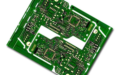
1、 Introduction: With the continuous improvement of human requirements for living environment, the environmental issues involved in the production process of PCB circuit boards are particularly prominent. The topic of lead and bromine is currently the most popular; Lead-free and halogen-free technologies will affect the development of PCB circuit boards in many ways. Although at present, the changes in the surface treatment process of circuit boards are not significant and may seem distant, it should be noted that long-term slow changes will lead to significant changes. With the increasing demand for environmental protection, the surface treatment process of PCB circuit boards is bound to undergo significant changes in the future. 2、 The purpose of surface treatment is to ensure good weldability or electrical performance, which is the most basic purpose of surface treatment. Due to the tendency of copper in nature to exist in the form of oxides in the air, it is unlikely to remai
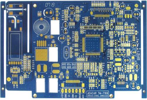
The holes on a circuit board are generally divided into copper holes and non copper holes. Non copper holes are mainly used for positioning and installation, and generally belong to larger holes with a diameter of 0.8mm or more. A through hole usually belongs to a plug-in or via hole, and the most common hole on a PCB board should be a via hole (conduction hole). The aperture of the plug-in hole is larger than the size of the via hole, usually above 0.5, based on the installation of capacitors, resistors, sockets, and other components. The main function of the electric hole is to conduct electricity, and the aperture is generally small, with a common aperture of less than 0.3. With the increase of precision boards, the functional requirements of the product increase, and the number of circuit board layers increases, the aperture is also getting smaller and smaller, with the minimum aperture of 0.1mm. Laser drilling is required. The through-hole needs to have a conductive effect, an
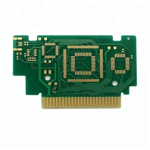
1. The surface of the welding area is contaminated, coated with flux, or metal compounds are generated on the surface of the SMT component. It can cause poor wetting. Sulfides on the surface of silver and oxides on the surface of tin can cause poor wetting. 2. When the residual metal in the solder exceeds 0.005%, the activity of the solder decreases and poor wetting occurs. 3. During wave soldering, there is gas on the surface of the substrate, which can also lead to poor wetting. The methods to solve poor wetting include: 1. Strictly implement the corresponding welding process. 2. PCB circuit boards and component surfaces should be cleaned properly. 3. Select the appropriate solder and set a reasonable welding temperature and time.
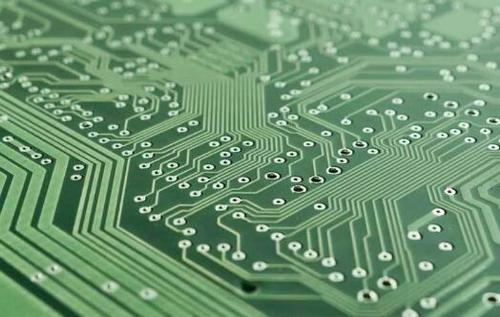
(1) Determine the variation pattern of the longitude and latitude direction and compensate it on the negative film according to the shrinkage rate (this work is carried out before photogrammetry). When cutting at the same time, process according to the fiber direction or according to the character markings provided by the manufacturer on the substrate (usually the vertical direction of the characters is the vertical direction of the substrate). When designing the circuit, it is important to ensure that the entire board surface is evenly distributed as much as possible. If it is not possible, it is necessary to leave a transition section in the space (without affecting the circuit position). This is due to the difference in warp and weft yarn density in the glass fabric structure of the board, resulting in differences in the warp and weft strength of the board. ⑶ Trial brushing should be used to keep the process parameters in a state, and then the rigid plate should be carried out
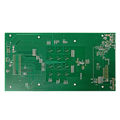
1. Preparation for welding: Preparation before welding includes cleaning of the welding area, installation of components, and preparation of solder, flux, and tools. Solder wire with the left hand and hold an electric soldering iron with the right hand (keep the soldering iron head clean and keep the soldering head in a welding state at all times). 2. Heating welding parts: Pay attention to heating the entire welding part evenly. 3. Feeding welding wire: After heating the weldment to a certain temperature, the welding wire and soldering iron come into contact with the weldment from the opposite side. 4. Remove the welding wire: When the welding wire melts a certain amount, immediately remove the welding wire. 5. Remove the soldering iron: After the soldering tin has moistened the welding pad or the welding part, remove the soldering iron. Manual soldering of PCB circuit boards is very simple for engineers who often weld them, but for those who have not welded them before, it m
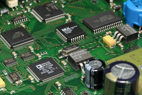
Some people have a strong interest in debugging PCB circuit boards, just like programmers solving bugs. There are many common PCB circuit board problems, including circuit board design, damage to electronic components, circuit shorts, component quality, and PCB circuit board wire breakage. Common PCB board failures mainly focus on components, such as capacitors, resistors, inductors, diodes, triodes, Field-effect transistor, etc. The integrated chips and crystal oscillators are obviously damaged, and the more intuitive way to judge these component failures can be observed through the eyes. There are obvious burning marks on the surface of electronic components with obvious damage. For faults like this, simply replacing the faulty component with a new one can solve the problem. Of course, not all electronic component damage can be observed with the naked eye, such as resistors, capacitors, transistors, etc. In some cases, the damage cannot be seen from the surface and requires the
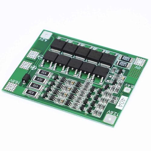
1. High heating device with heat sink and heat conduction plate When there are a few components in the PCB that have a high heat output (less than 3), a heat sink or heat transfer tube can be added to the heating device. When the temperature cannot be lowered, a heat sink with a fan can be used to enhance the heat dissipation effect. When there are a large number of heating devices (more than 3), a large heat dissipation cover (board) can be used. It is a specialized heat sink customized according to the position and height of the heating devices on the PCB board, or different component high and low positions can be cut out on a large flat heat sink. Snap the heat dissipation cover onto the surface of each component as a whole and dissipate heat by contacting each component. However, due to poor consistency in height during component assembly and welding, the heat dissipation effect is not good. Generally, soft thermal phase change Thermally conductive pad is added on the surface
The direct reason for the temperature rise of printed boards is due to the presence of circuit power consuming devices. Electronic devices have varying degrees of power consumption, and the heating intensity varies with the size of power consumption. Two phenomena of temperature rise in printed boards: (1) Local or large-scale temperature rise; (2) Short term or prolonged temperature rise. When analyzing the thermal power consumption of PCB circuit boards, it is generally analyzed from the following aspects. 1. Electrical power consumption (1) Analyze the power consumption per unit area; (2) Analyze the distribution of power consumption on PCB circuit boards. 2. Structure of printed boards (1) The size of the printed board; (2) The material of the printed board. 3. Installation method of printed boards (1) Installation method (such as vertical installation, horizontal installation); (2) Sealing condition and distance from the casing.
Inquiry Now

