 +86 755 2794 4155
  sales@knownpcb.com
-
Shenzhen KNOWNPCB Technology Co., Ltd.
 +86 755 2794 4155
  sales@knownpcb.com
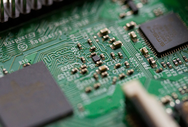
Have you noticed that now more and more of our lighting is using led lighting.What is LED? Compared to the traditional light bulbs, LEDs have lower power consumption, longer lifetime and higher energy efficiency. In the PCB industry,when we say LED PCB, it refers to the pcb used for LED lighting, if you are looking for a suitable LED PCB for your lighting system, this article may bring you something. WHAT ARE LEDS COMPOSED OF?LED is an initial light-emitting diode that produces light when an electric current passes through. LEDs typically have negative and positive electrodes, which generate light in the visible light region.The LEDS are glued to the PCB by soldering process and have electrical connections for lighting.Since light-emitting diodes dissipate a lot of heat when they are in use, when you are designing LED, the metal core is usually the best choice for LED PCB, it is because that it dissipates heat more faster. Among them, the metal material aluminum is the most widely used
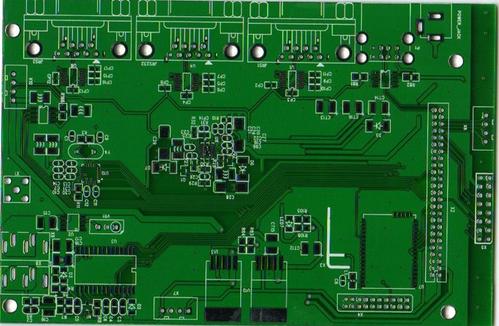
Printed circuit boards are the most active industry in the contemporary electronic component industry, and their industry growth rate is generally about 3 percentage points higher than that of the electronic component industry. It is expected to maintain rapid growth in 2006, with demand upgrading and industrial transfer being the basic driving forces for industry development, while varieties such as HDI boards, flexible boards, and IC packaging boards (BGA, CSP) will become the main growth points. In 2003, the output value of printed circuit boards in China was 50.069 billion yuan, a year-on-year increase of 333%, surpassing the second largest in the world, the United States, for the first time. In 2004 and 2005, China's PCB output value still maintained a growth rate of over 30%, estimated to reach 86.9 billion yuan in 2005, far exceeding the growth rate of the global industry. Flexible circuit boards are rapidly developing towards miniaturization in electronic devices represen
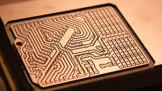
The suitability of PCB circuit boards in terms of system signal, connection distance, and capacitive load is considered before deciding whether to use transmission lines. What types of transmission lines are commonly used in PCB circuit boards? The main types of transmission lines for PCB circuit boards are: (1) Coaxial cables and twisted pair cables: They are often used for the connection between PCB circuit board transmission systems and systems. The characteristic impedance of coaxial cables is typically 50 Ω and 75 Ω, while twisted pair cables are typically 110 Ω. (2) Microstrip on PCB The Microstrip is a strip conductor (signal line). It is separated from the ground plane by a dielectric. If the thickness, width, and distance from the ground plane of a line are controllable, its characteristic impedance can also be controlled. (3) Strip lines in printed boards A strip line is a copper strip line placed between two conductive planes in the middle of a dielectric medium. I
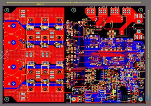
1. Pad design (1) When designing plug-in component pads, the pad size should be designed appropriately. If the solder pad is too large, the solder spreading area is large, and the formed solder joints are not full, while the surface tension of the smaller solder pad copper foil is too small, and the formed solder joints are non wetting solder joints. The fit gap between the aperture and the component lead is too large, which is prone to false soldering. When the aperture is 0.05-0.2mm wider than the lead and the diameter of the solder pad is 2-2.5 times the aperture, it is an ideal welding condition. (2) When designing solder pads for SMD components, the following points should be considered: in order to eliminate the "shadow effect" as much as possible, the solder end or pin of SMD should be facing the direction of the tin flow to facilitate contact with the tin flow and reduce false soldering and solder leakage. For smaller components, they should not be placed behind larger co
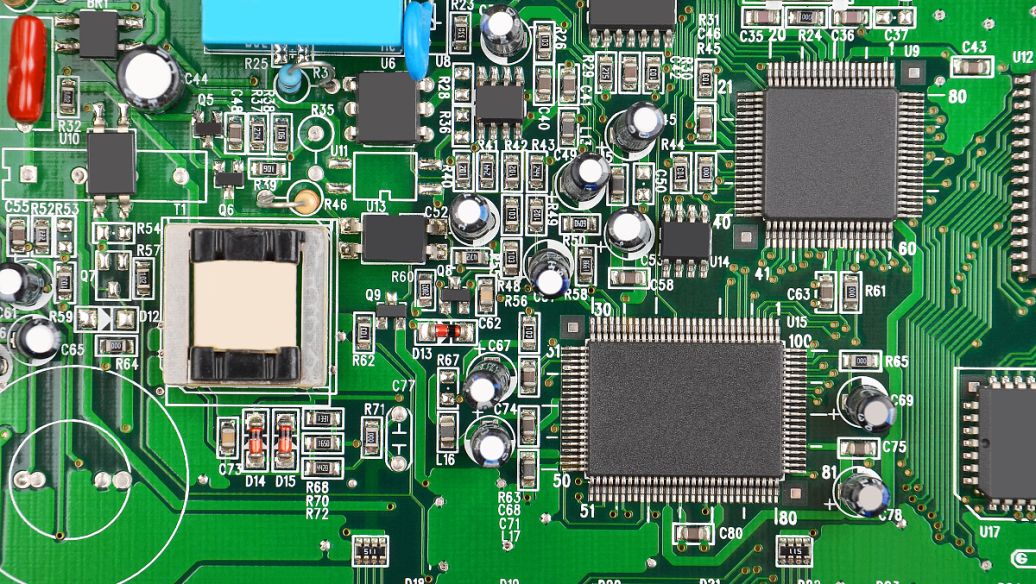
Sometimes, PCB circuit board substrates can cause open circuits, which are mainly caused by: 1. There are scratches on the copper clad plate before entering the warehouse; 2. The copper clad plate was scratched during the cutting process; 3. The copper clad plate was scratched by the drilling nozzle during drilling; 4. The copper clad plate was scratched during transportation; 5. The surface copper foil was damaged due to improper operation during the stacking of boards after copper deposition; 6. The copper foil on the surface of the production board was scratched when passing through the leveling machine. Improvement methods: 1. Before entering the warehouse, the IQC must conduct spot checks on the copper clad PCB circuit board substrate to check if there are scratches or exposed substrate on the board surface. If there are any, the supplier should be contacted in a timely manner to make appropriate treatment based on the actual situation. 2. The PCB circuit board substr
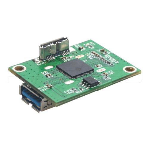
After decades of development, the PCB circuit board industry has become extremely mature in terms of technology. Key technologies such as drilling, copper deposition, exposure, development, and etching have been well controlled by automation equipment, making PCB circuit board factories an equipment and fixed asset intensive industry. Business owners have to come up with low price strategies in the fierce market competition. Therefore, the market will be full of the phenomenon of Gresham's law. How to stand out from fierce market competition? It is worth every manager's deep thinking.The rise of any industry is first about creativity, then about the market, and finally about quality. At the beginning, insightful individuals will first identify potential market opportunities, enter the market first, and quickly gain profits. Then more and more people will discover such business opportunities and enter the market competition. Finally, when the industry is saturated, end customers can fre

The competition of enterprises is diversified, from the previous short Plate theory theory to the current long Plate theory theory. Faced with fierce market competition, limited resources of enterprises can only be concentrated on a certain board, making it bigger and stronger. This has led many electronic product companies to only focus on research and development and sales, outsourcing PCBA electronic manufacturing to professional companies, and no longer trying out material procurement, outsourcing processing, supply chain management, and so on that they are not good at. The benefit of doing so is to reduce manpower investment and management costs, as well as the risk losses caused by one's lack of expertise. Careful people will find that in recent years, more and more companies have begun to seek professional PCBA electronic manufacturing resources.Another driving factor is the country's advocacy for mass entrepreneurship and innovation, which has led to an increasing number of sma
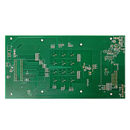
(1) Although the wiring spacing and wiring width are consistent, the spacing of Coupon Test point is fixed at 2.54mm (to meet the spacing of test probes), and the spacing of the end of the actual wiring in the board (i.e., the golden finger) is variable. With the emergence of QFP, PLCC, and BGA packages, the pin spacing of some chips is far less than 2.54mm (i.e., the spacing of Coupon Test point).(2) Coupon wiring is an ideal straight line, while the actual wiring on the board is often designed and produced according to actual needs. PCB designers and production personnel can easily idealize Coupon's wiring, but the actual wiring on the PCB board may undergo irregular changes due to practical needs.(3) The positions of Coupon and the actual wiring inside the board are different on the entire PCB board. Coupons are located in the middle or edge of the PCB board and are often removed by the manufacturer when the PCB board leaves the factory. The actual positions of the wiring inside the
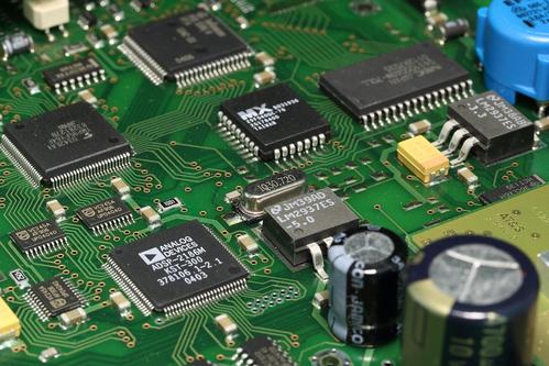
(1) The distance between the Test point of Coupon is different from that of the cabling of Coupon, which will cause impedance discontinuity between the Test point and the cabling. This will result in different impedance test results.(2) The impedance changes reflected by curved wiring and ideal wiring are inconsistent. The characteristic impedance at the bending and turning point of the wiring is often discontinuous, while Coupon's idealized wiring cannot reflect the impedance discontinuity caused by the bending of the wiring.(3) Coupon and real wiring have different positions on the PCB board. Currently, PCB boards are designed with multi-layer wiring and require pressing during production. When a PCB board is pressed, the pressure on different positions of the board cannot be consistent, and the thickness of the dielectric layer at different positions will also vary. As a result, the dielectric constant of the PCB board made from this method often varies at different positions, and t
Inquiry Now

