 +86 755 2794 4155
  sales@knownpcb.com
-
Shenzhen KNOWNPCB Technology Co., Ltd.
 +86 755 2794 4155
  sales@knownpcb.com
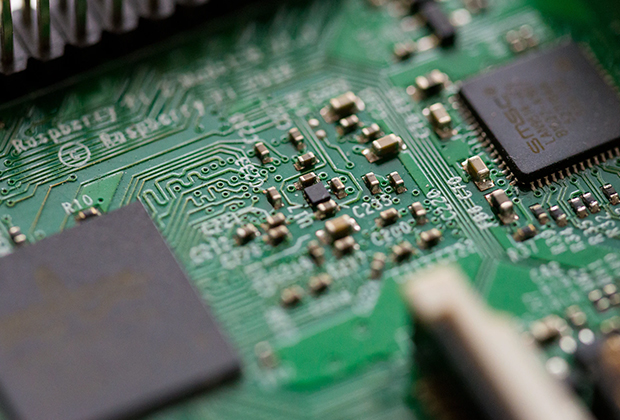
Have you noticed that now more and more of our lighting is using led lighting.What is LED? Compared to the traditional light bulbs, LEDs have lower power consumption, longer lifetime and higher energy efficiency. In the PCB industry,when we say LED PCB, it refers to the pcb used for LED lighting, if you are looking for a suitable LED PCB for your lighting system, this article may bring you something. WHAT ARE LEDS COMPOSED OF?LED is an initial light-emitting diode that produces light when an electric current passes through. LEDs typically have negative and positive electrodes, which generate light in the visible light region.The LEDS are glued to the PCB by soldering process and have electrical connections for lighting.Since light-emitting diodes dissipate a lot of heat when they are in use, when you are designing LED, the metal core is usually the best choice for LED PCB, it is because that it dissipates heat more faster. Among them, the metal material aluminum is the most widely used
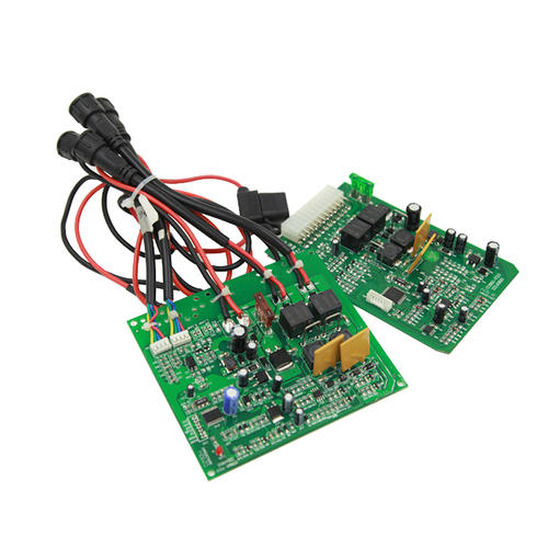
The memory packaged with BGA technology can increase the memory capacity by two to three times without changing its volume. Compared with TSOP, BGA has smaller volume, better heat dissipation performance, and electrical performance. BGA packaging technology has greatly improved the storage capacity per square inch. Memory products using BGA packaging technology have a volume of only one-third that of TSOP packaging at the same capacity; In addition, compared to traditional TSOP packaging methods, BGA packaging has a faster and more effective heat dissipation path. The I/O terminals of BGA packaging are distributed in an array of circular or columnar solder joints below the packaging. The advantage of BGA technology is that although the number of I/O pins increases, the pin spacing does not decrease but increases, thereby improving the assembly yield; Although its power consumption increases, BGA can be soldered using a controllable collapse chip method, which can improve its electro

As soon as BGA emerged, it became the best choice for high-density, high-performance, multifunctional, and high I/O pin packaging of VLSI chips such as CPUs and north-south bridges. Its characteristics include: Although the number of I/O pins has increased, the pin spacing is much greater than that of QFP, thereby improving the assembly yield; Although its power consumption increases, BGA can be soldered using the controllable collapse chip method, abbreviated as C4 soldering, which can improve its electric heating performance; 3. The thickness is reduced by more than 1/2 compared to QFP, and the weight is reduced by more than 3/4; 4. The parasitic parameters are reduced, the signal transmission delay is small, and the usage frequency is greatly increased; 5. Assembly can be carried out using coplanar welding, with high reliability; 6. BGA packaging is still the same as QFP and PGA, occupying too much substrate area; Intel Corporation adopts ceramic pin grid array packaging

1. PBGA (Plastic BGA) substrate: Generally a multi-layer board composed of 2-4 layers of organic materials. In the Intel series of CPUs, Pentium II, III, and IV processors all adopt this packaging form. In the past two years, another form has emerged: directly binding ICs to boards, which are much cheaper than regular prices and are generally used in fields such as games that do not have strict quality requirements. 2. CBGA (CeramicBGA) substrate: refers to a ceramic substrate, and the electrical connection between chips and substrates is usually installed using FlipChip (FC). In the Intel series of CPUs, Pentium I, II, and Pentium Pro processors have all adopted this packaging form. 3. FCBGA (FilpChipBGA) substrate: Hard multilayer substrate. 4. TBGA (TapeBGA) substrate: The substrate is a ribbon soft 1-2 layer PCB circuit board. 5. CDPBGA (Carity Down PBGA) substrate: Refers to the chip area (also known as the cavity area) with a square depression in the packaging center.
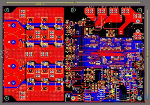
The substrate or intermediate layer is a very important part in BGA packaging. In addition to being used for interconnection wiring, it can also be used for impedance control and integration of inductors, resistors, and capacitors. Therefore, the substrate material is required to have high Glass transition temperature rS (about 175~230 ℃), high dimensional stability, low moisture absorption, good electrical performance and high reliability. The metal film, insulation layer, and substrate medium also have high adhesion performance. 1. Packaging process flow of PBGA wire bonding ① Preparation of PBGA substrate Laminate extremely thin (12-18) on both sides of BT resin/glass core board μ M thick copper foil, followed by drilling and through hole metallization. Create graphics on both sides of the substrate using conventional PCB and 3232 technology, such as guide strips, electrodes, and solder zone arrays for installing solder balls. Then add a solder mask and create a pattern to ex
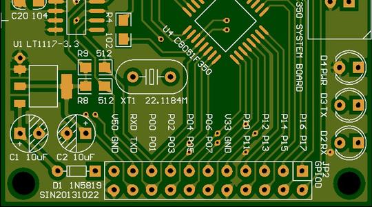
QFN is a kind of non -quoted feet packaging, which is square or rectangular. There is a large -area naked pad in the center of the packaging at the center of the packaging to conduct heat. The electrical conductivity pad with electrical links around the packaging periphery around large pads. Because QFN packaging does not have gull -wing -like leads like the traditional SOIC and TSOP packaging, the conductivity between the internal pins and the pads is short, the self -sense coefficient and the wiring resistance in the packaging body are very low, so it can provide excellent electrical properties. In addition, it also provides excellent heat dissipation performance through the exposed lead frame pad. The pad has a direct cooling channel to release the heat in the package. The heat dissipation pad is usually welded directly on the circuit board, and the heat dissipation of the PCB can help spread the excess power consumption to the copper connecting floor, thereby absorbing excess h
The thickness of the mesh board determines the amount of welded paste printing on PCB. Too many welded paste will cause the bridge to connect when the return welding. Therefore, it is recommended that the QFN package of 0.5mm spacing uses a net board with a thickness of 0.12mm thickness and a 0.65mm spacing QFN packaging with a net board with a thickness of 0.15mm. It is recommended that the mesh opening size can be appropriately smaller than the pad to reduce the occurrence of the welded bridge connection. As shown in Figure 5. (2) Netboard design of heat dissipation pads When welding the exposed pads at the bottom of the chip and the hot pads on the PCB, the gas in the pores and the gas in large -sized pads will overflow due to the heat pores and large -sized pads. All kinds of defects (such as sputtering, welding balls, etc.), but it is almost impossible to eliminate these pores, only reduce the pores to the lowest amount. Therefore, in the design of the mesh area of the hot pa
Because the qfn's solder joints are below the packaging body, and the thickness is thin, X -Ray cannot detect the QFN solder point less tin and the opening of the road. It can only be judged as possible by the external welding joint situation. However, the current QFN welding The determination standards of the point part of the point part of the side have not yet appeared in the IPC standard. With no more ways for the time being, the testing stations that rely on post -production will be relying on the after -production section to judge the quality of welding. From the X -Ray images in Figure 6, the difference between the side part is obvious, but the image of the bottom part of the performance of the welding point performance is the same, so this brings problems to the X -ray detection and judgment. The use of electric iron to add tin, which increases only the side part, which impacts on the bottom part, X -Ray still cannot judge. Judging from the local magnifying of the appearan
For the repairs of QFN, because the welding point is completely at the bottom of the component packaging, any defects such as bridges, roads, and tin balls need to be moved away, so it is somewhat similar to the repairs of BGA. QFN is small in size, light weight, and they are used on high -density assembly boards, making it more difficult to repairs than BGA. At present, QFN repairs are still a part of the urgent development and improvement of the entire surface installation process. In particular, it is necessary to use welded paste A reliable electrical and mechanical connection between QFN and the printed board is indeed difficult. At present, there are three kinds of feasible coating ointments: one is to use the traditional use of the small silk net printing solder balla Print the welding balm directly on the pad of the component. The above methods need to be very skilled to repair the workers to complete this task. The choice of repairs equipment is also very important. It mu
Inquiry Now

