 +86 755 2794 4155
  sales@knownpcb.com
-
Shenzhen KNOWNPCB Technology Co., Ltd.
 +86 755 2794 4155
  sales@knownpcb.com
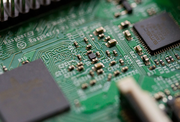
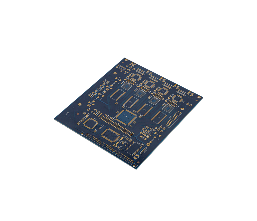
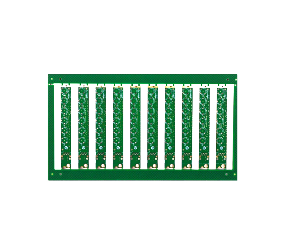
Have you noticed that now more and more of our lighting is using led lighting.What is LED? Compared to the traditional light bulbs, LEDs have lower power consumption, longer lifetime and higher energy efficiency. In the PCB industry,when we say LED PCB, it refers to the pcb used for LED lighting, if you are looking for a suitable LED PCB for your lighting system, this article may bring you something. WHAT ARE LEDS COMPOSED OF?LED is an initial light-emitting diode that produces light when an electric current passes through. LEDs typically have negative and positive electrodes, which generate light in the visible light region.The LEDS are glued to the PCB by soldering process and have electrical connections for lighting.Since light-emitting diodes dissipate a lot of heat when they are in use, when you are designing LED, the metal core is usually the best choice for LED PCB, it is because that it dissipates heat more faster. Among them, the metal material aluminum is the most widely used
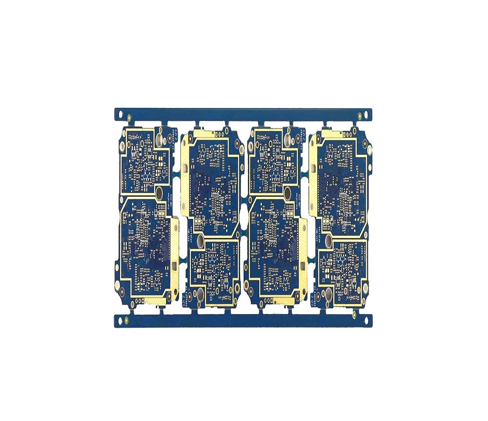
PCB board fixture is a detection device for PCB boards, especially a fixture for PCB board detection. There is a fixed seat set on the machine base that can slide back and forth, a front gear lever and a rear gear lever set on the fixed seat. The front gear lever is fixedly connected to the fixed seat, and the rear gear lever is slidably connected to the fixed seat. The front gear lever is equipped with a PCB board clamp head composed of a warping plate and a top plate, and the middle part of the PCB board clamp head is connected to the front gear lever pin, and a top rod device is set at the front end of the machine base, The top rod device is composed of a base fixed on the machine base and a top rod set on the base. When the fixed base moves to the forefront, the top rod of the top rod device contacts the top plate. The utility model has a simple structure and can conveniently and quickly clamp the PCB board, improving work efficiency. At the same time, the clamping of the PCB b
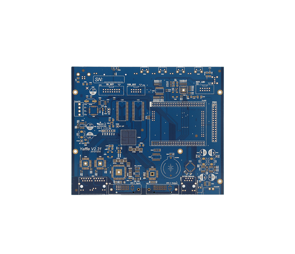
Panel length: 330mm Overall dimensions: 700 x 230 x 420 Panel thickness: 0.3-3.5 mm Machine weight 165kg 1. Fully pneumatic control, no noise 2. Small travel, less prone to product damage, and safe operation 3. Tailored work, suitable for various thicknesses of PCB 4. Minimize the internal stress generated during plate cutting to avoid tin cracking 5. The distance between the upper and lower knives can be accurately adjusted, avoiding tool loss due to different depths of the V-groove 6. The highest part at the edge of the separable V-groove is 70mm
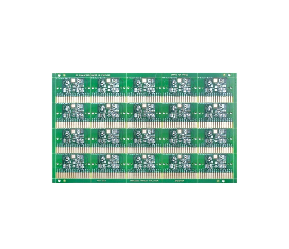
Computer and peripherals: motherboard, monitor, network card, memory card, IC, mouse, router, camera, USB drive, fan motor, game console, game card board (gold finger board) Mobile phone: mobile phone board, charger electronic anti-theft lock audio, printer, copier, fax machine, phone, scanner monitoring system, video head DV, camera meter board Automotive products: Sensors for various machines such as car audio, air conditioning switches, control system lighting fixtures, LED panels (LCD displays, LCD billboards) Bathroom equipment: motors, controllers, switches, and high-end PCB boards in industries such as medical equipment, military equipment, aerospace equipment, etc
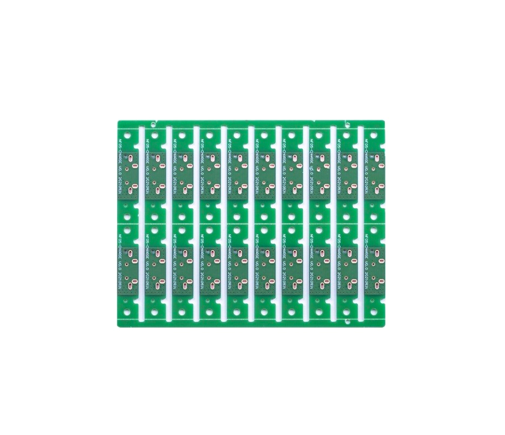
Double-sided PCB board is a very important type of PCB board in the circuit board market. There are double-sided circuit boards with metal base, Hi Tg heavy copper foil circuit boards, flat and winding double-sided circuit boards, high-frequency PCBs, mixed dielectric base high-frequency double-sided circuit boards, etc. It is suitable for a wide range of high-tech industries such as telecommunications, power supply, computers, industrial control, digital products, scientific and educational instruments, medical equipment, automobiles, aerospace defense, etc. Double-sided printed boards are usually made of epoxy glass cloth copper foil. It is mainly used for communication electronics with high performance requirements Equipment, advanced instruments and electronic computers, etc. The production process of double-sided boards is generally divided into several types: process wire method, hole blocking method, masking method, and graphic electroplating etching method. The process f
Square solder pads are commonly used when the components on a printed board are large but few, and the printed wires are simple. When manually making PCBs, using this type of solder pad is easy to achieve. Circular pad - widely used in single and double-sided printed boards with regular component arrangement. If the density of the board allows, the solder pad can be larger to prevent detachment during welding. Island shaped pad - The connection between the pad and the pad is integrated. Commonly used in vertical irregular arrangement installation. For example, this type of pad is often used in tape recorders. Teardrop solder pads - often used when the wire connecting the pads is thin to prevent peeling and disconnection of the wire from the pads. This type of pad is commonly used in high-frequency circuits. Polygonal pad - used to distinguish pads with similar outer diameters but different apertures, making it easy to process and assemble. Elliptical pads - These pads have suff
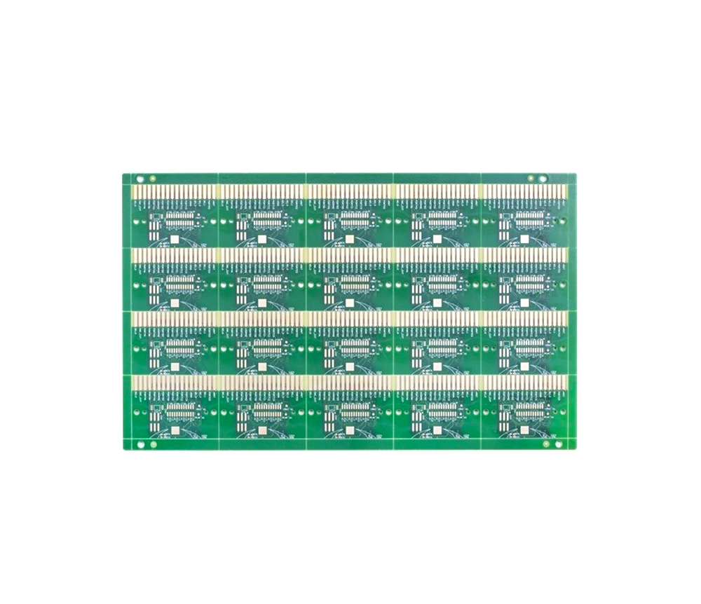
Copper clad panels were truly adopted on a large scale in PCB production, first appearing in the US PCB industry in 1947. The PCB substrate material industry has also entered its early stage of development. During this stage, the manufacturing technology progress of the raw materials used in the manufacturing of substrate materials - organic resins, reinforcing materials, copper foil, etc. - provides a strong driving force for the development of the substrate material industry. As a result, the manufacturing technology of substrate materials is gradually maturing. The invention and application of integrated circuits, as well as the miniaturization and high-performance of electronic products, have pushed PCB substrate material technology onto the track of high-performance development. The rapid expansion of demand for PCB products in the world market has led to rapid development in the production, variety, and technology of PCB substrate materials. At this stage, a broad new field
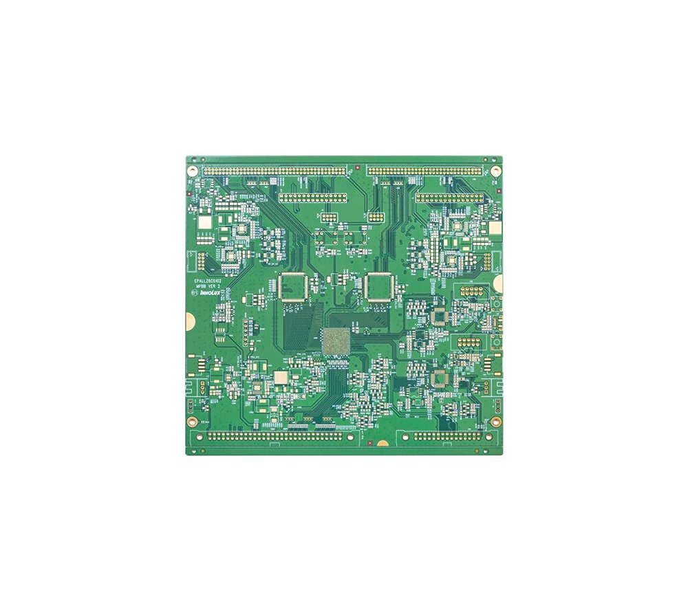
1. Drilling machine: used for drilling circuit boards. 2. Nailing machine: Fix or stack one or more double-sided boards with pipe position nails to facilitate positioning during drilling. 3. Grinding drill bit machine: The drill bit used for grinding and drilling. 4. Up and down rubber granulator; Fix the length of the rubber particles dropped from the drilling nozzle at 0.800 "± 0.005" for use by the drilling rig, or remove the rubber particles from the drilling nozzle. 5. Nail withdrawing machine; Use double-sided board drilling to retract pipe position nails. 6. Drilling machine: Used for drilling pipe position holes on the bottom plate.
1.1. When the cutting machine is turned on, do not reach into the machine. 2.2. Flammable materials such as paper should not be placed next to the oven to prevent fires. 3.3. The temperature setting of the oven must not exceed the specified value. 4.4. Asbestos gloves must be worn when removing boards from the oven, and the boards must be removed after they have cooled down. 5.5. Dispose of waste materials strictly according to the method specified in MEI001 to prevent environmental pollution. Cutting board 1. Equipment: manual plate cutting machine, target milling machine, CCD Hole punch, gong machine, edging machine, word marking machine, thickness gauge; 2. Function: Laminate shape processing, preliminary forming; Process: Dismantling board → Dotting and drawing lines → Cutting large board → Milling copper skin → Punching → Forming gong edge → Grinding edge → Typing mark → measuring plate thickness
Inquiry Now

