 +86 755 2794 4155
  sales@knownpcb.com
-
Shenzhen KNOWNPCB Technology Co., Ltd.
 +86 755 2794 4155
  sales@knownpcb.com
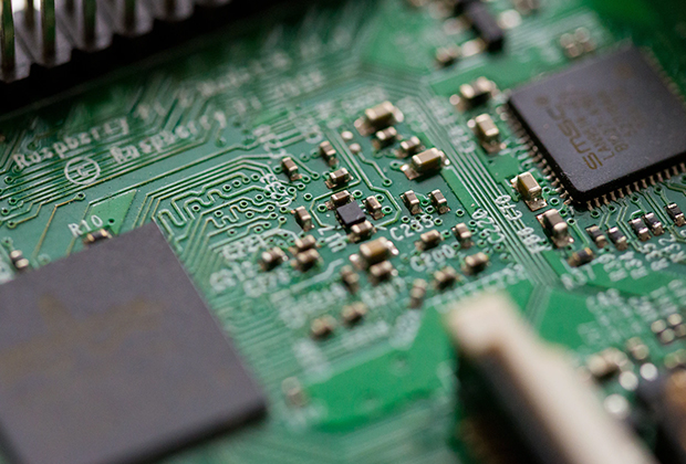
Have you noticed that now more and more of our lighting is using led lighting.What is LED? Compared to the traditional light bulbs, LEDs have lower power consumption, longer lifetime and higher energy efficiency. In the PCB industry,when we say LED PCB, it refers to the pcb used for LED lighting, if you are looking for a suitable LED PCB for your lighting system, this article may bring you something. WHAT ARE LEDS COMPOSED OF?LED is an initial light-emitting diode that produces light when an electric current passes through. LEDs typically have negative and positive electrodes, which generate light in the visible light region.The LEDS are glued to the PCB by soldering process and have electrical connections for lighting.Since light-emitting diodes dissipate a lot of heat when they are in use, when you are designing LED, the metal core is usually the best choice for LED PCB, it is because that it dissipates heat more faster. Among them, the metal material aluminum is the most widely used
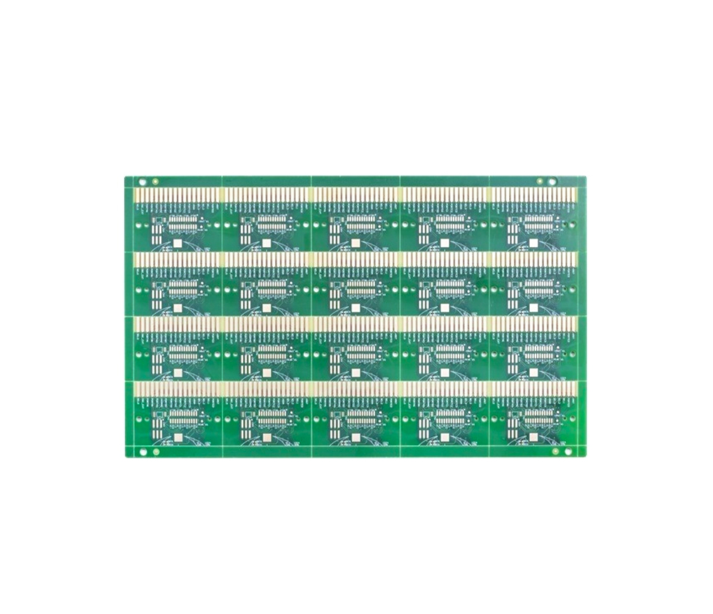
PCB upper shelf PCB loading rack, also known as PCB collection box, PCB automatic loading rack, SMT loading and unloading rack, etc. Widely applicable to automatic loading and unloading machines, it is acid resistant, oil resistant, high temperature resistant, non-toxic, and odorless. It can be used to hold PCB boards, making cleaning convenient, circuit board turnover convenient, stacking neatly, and easy to manage. Its reasonable design and excellent quality are suitable for transportation, distribution, storage, circulation and processing in factories. The SMT loading and unloading rack can be combined with various logistics containers and workstations, and is used in various warehouses, production sites, and other occasions. In today's world where automatic loading and unloading machines are increasingly valued by enterprises, the SMT loading and unloading rack helps complete the circulation, storage, and integrated management of PCB boards. It is a necessary product for modern

PCB upper shelf according to size 1. External dimensions: 355 * 315 * 580mm, can store 50 PCB boards. PCB board specifications: 350 * (80-250) mm PCB upper shelf Side plate guide groove. The groove depth is 3.5mm, the groove width is 8mm, and the pitch is 10mm 2. External dimensions: 355 * 320 * 563mm. Can store 50 PCB boards. PCB board specifications: 350 * (50-250) mm Side plate guide groove. The groove depth is 3.5mm, the groove width is 5mm, and the pitch is 10mm 3. External dimensions: 460 * 400 * 563mm. Can store 50 PCB boards. PCB board specifications: 460 * (100-330) mm Side plate guide groove. Groove depth 3.5mm, groove width 5mm, pitch 10mm 4. External dimensions: 535 * 460 * 570mm, can store 50 PCB boards. PCB board specifications: 535 * (50-390) mm Side plate guide groove. The groove depth is 3.5mm, the groove width is 5mm, and the pitch is 10mm.
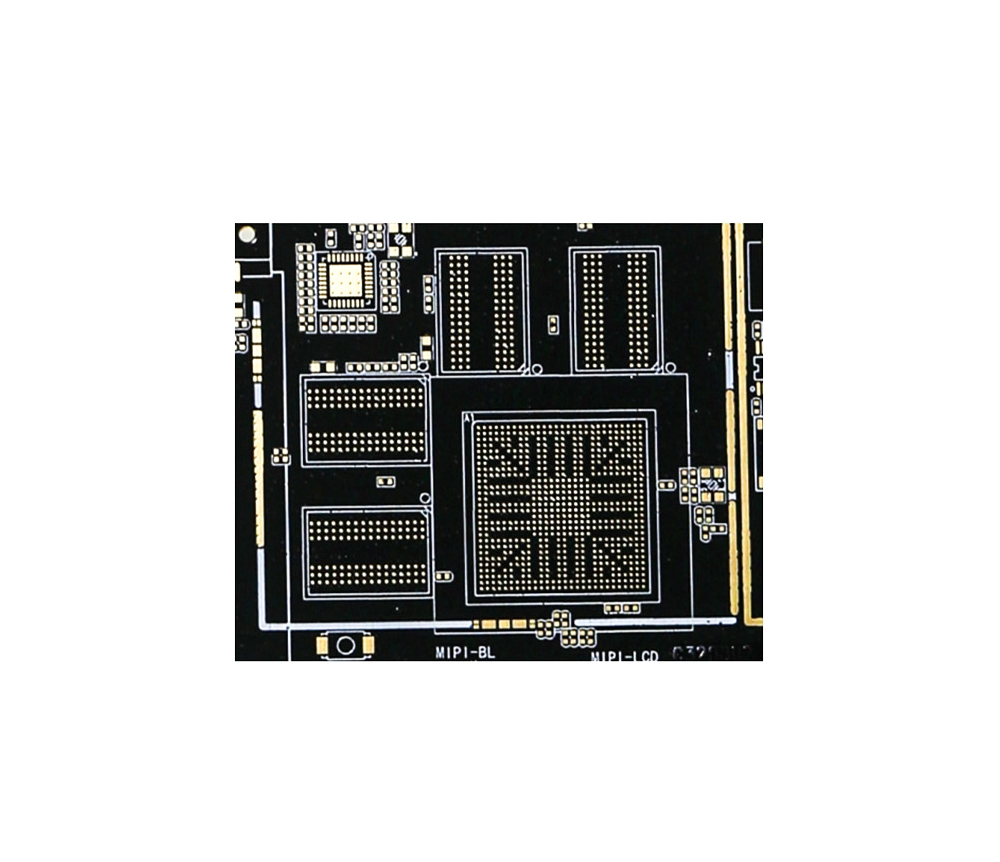
Classified by the upstream and downstream of the industrial chain, it can be divided into raw materials - copper clad panels - printed circuit boards - electronic product applications. The relationship is simply expressed as: fiberglass cloth: fiberglass cloth is one of the raw materials of copper clad panels, made from fiberglass yarn weaving, accounting for about 40% (thick plate) and 25% (thin plate) of the cost of copper clad panels. Glass fiber yarn is made by calcining raw materials such as silica sand in a kiln into a liquid state. It is then pulled into extremely fine glass fibers through extremely small alloy nozzles, and then hundreds of glass fibers are twisted into glass fiber yarn. The construction investment of kilns is huge, usually requiring billions of funds, and once ignited, production must be uninterrupted 24 hours a day, resulting in huge exit costs. Fiberglass fabric manufacturing is similar to weaving enterprises in that it can control production capacity and q
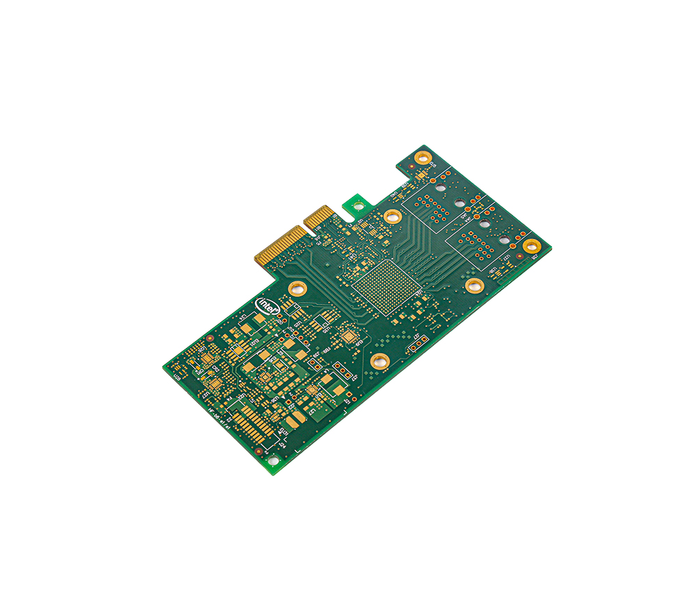
The global PCB industry accounts for more than a quarter of the total output value of the electronic component industry, and is the industry with the largest proportion among various electronic component sub industries, with an industry scale of 40 billion US dollars. Meanwhile, due to its unique position in the electronic basic industry, it has become the most active industry in the contemporary electronic component industry. In 2003 and 2004, the global PCB output value was 34.4 billion US dollars and 40.1 billion US dollars, with year-on-year growth rates of 5.27% and 16.47%, respectively. Development status of domestic PCB industry The PCB development work in China began in 1956 and gradually expanded to form the PCB industry from 1963 to 1978. After more than 20 years of reform and opening up, due to the introduction of advanced foreign technology and equipment, single panel, double-sided board, and multi-layer board have all achieved rapid development, and the domestic PCB i
In the early years, circuit boards belonged to the high-tech industry, and most foreign companies controlled technology output, which at one time constrained and restricted the development and growth of the circuit board industry. According to Time magazine, China and India are among the most polluted countries in the world. To protect the environment, the Chinese government has been strictly formulating and implementing relevant pollution control regulations, which have affected the PCB industry. Many cities and towns are no longer allowed to expand and build new PCB factories, but the development of our circuit board enterprises is now restricted by local conditions. The more economically developed the areas, the greater the restrictions. Why? Because unconsciously, circuit board enterprises have developed into what the government sees as major polluters, energy consumers, and water users! In today's society where environmental protection and sustainable development are highly va
Frequently Asked Questions 1、 Degreasing (temperature 60-65 ℃) 1. Too much foam: abnormal quality caused by too much foam: poor degreasing effect, caused by mismatched bath solution. 2. Composition of particulate matter: The reason for the composition of particulate matter is that the filter is broken, the high-pressure water washing of the grinding machine is insufficient, and dust is brought in from the outside. 3. Finger prints cannot be degreased: Finger prints cannot be degreased due to low degreasing temperature and incorrect dispensing of medication. 2、 Micro corrosion (NPS 80-120G/L H2SO4 5% temperature 25-35 ℃) 1. The copper surface of the board is slightly white: the reason is due to insufficient grinding, oil removal, or contamination, and low concentration of liquid medicine. 2. The copper surface of the board is black: it cannot be washed clean after oil removal and is contaminated by oil removal. A pink surface on copper indicates a normal effect of micro etchi

1. Copper foil is excessively etched, and the electrolytic copper foil used in the market is generally single-sided galvanized (commonly known as ashed foil) and single-sided copper plated (commonly known as reddened foil). The common copper throwing is generally galvanized copper foil above 70um, while reddened foil and ashed foil below 18um have not undergone bulk copper throwing. 2. Local collisions occurred during the PCB process, causing the copper wire to detach from the substrate due to external mechanical forces. This defect manifests as poor positioning or directionality, where the detached copper wire will have obvious twisting or scratches/impact marks in the same direction. Peel off the defective copper wire and observe the rough surface of the copper foil. It can be seen that the color of the rough surface of the copper foil is normal, and there will be no side corrosion defects. The peeling strength of the copper foil is normal. 3. Unreasonable PCB circuit design, u

1. Engineering design: The arrangement of interlayer semi cured sheets should correspond; Multi layer core boards and semi cured sheets should use the same supplier's products; The outer C/S surface graphics area should be as close as possible, and independent grids can be used; 2. Drying board before cutting Generally, at 150 degrees Celsius for 6-10 hours, the moisture inside the board is removed, further allowing the resin to cure completely and eliminating stress inside the board; Drying the board before opening, both the inner layer and both sides are required! 3. Before laminating the multi-layer board, attention should be paid to the longitudinal and latitudinal directions of the cured sheet: The shrinkage ratio in the warp and weft directions is different, so pay attention to distinguishing the warp and weft directions before cutting and stacking the semi cured sheet; When cutting the core board, attention should also be paid to the warp and weft directions; The gener
Inquiry Now

