 +86 755 2794 4155
  sales@knownpcb.com
-
Shenzhen KNOWNPCB Technology Co., Ltd.
 +86 755 2794 4155
  sales@knownpcb.com
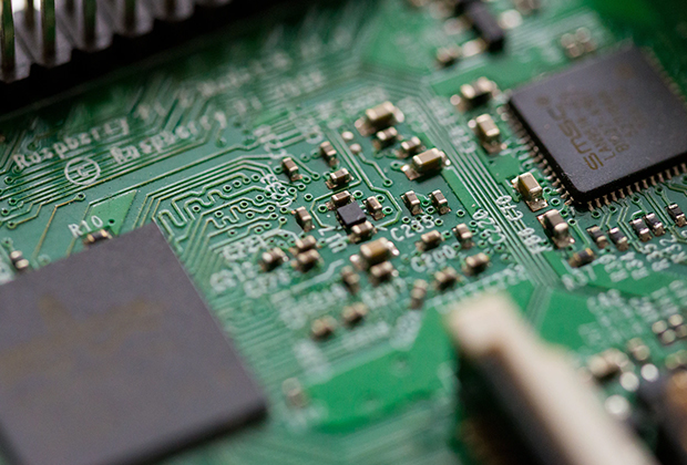
Have you noticed that now more and more of our lighting is using led lighting.What is LED? Compared to the traditional light bulbs, LEDs have lower power consumption, longer lifetime and higher energy efficiency. In the PCB industry,when we say LED PCB, it refers to the pcb used for LED lighting, if you are looking for a suitable LED PCB for your lighting system, this article may bring you something. WHAT ARE LEDS COMPOSED OF?LED is an initial light-emitting diode that produces light when an electric current passes through. LEDs typically have negative and positive electrodes, which generate light in the visible light region.The LEDS are glued to the PCB by soldering process and have electrical connections for lighting.Since light-emitting diodes dissipate a lot of heat when they are in use, when you are designing LED, the metal core is usually the best choice for LED PCB, it is because that it dissipates heat more faster. Among them, the metal material aluminum is the most widely used
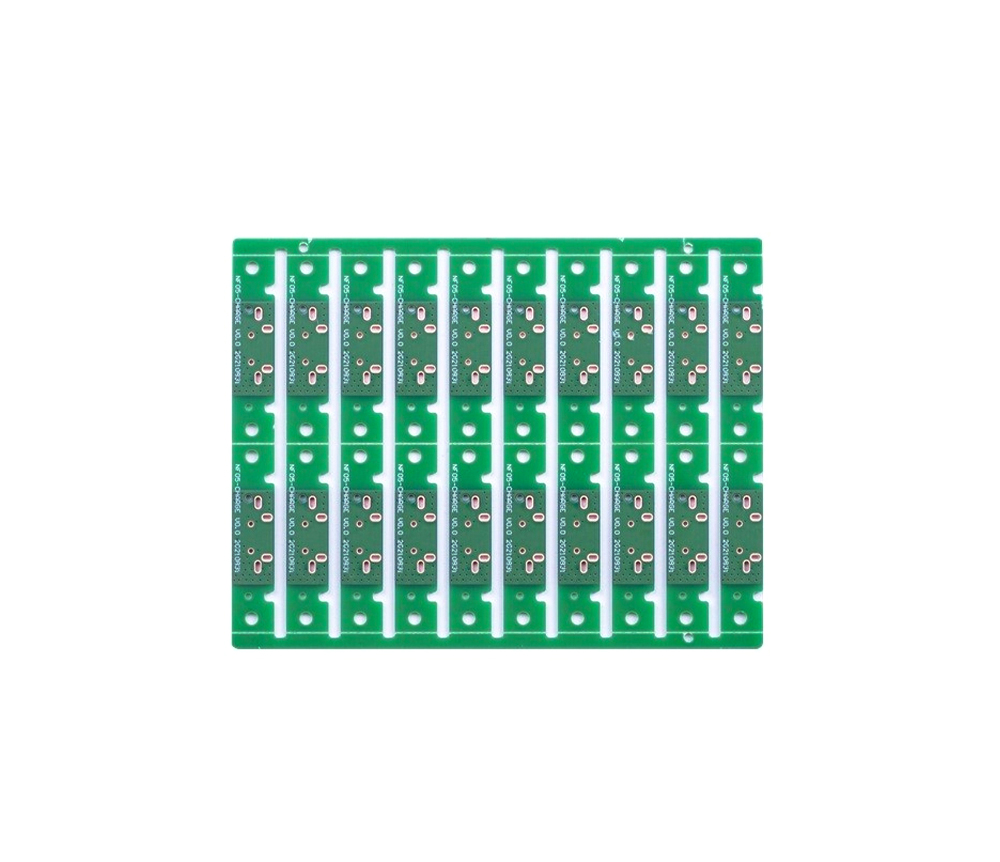
During the production process, the problem of being scrapped and replenished in order to prevent too low or reduce the problem of excessive rates of drilling, pressure delay, and cutting in order to prevent too much short circuit. The best effect of the best effect is particularly important before giving birth. Pre -treatment of pre -treatment, there are three aspects that need to be dealt with. These three aspects are completed by engineers. The first is the FPC board engineering evaluation, mainly to evaluate whether the customer’s FPC board can produce, whether the company's production capacity can meet the customer's board requirements and unit costs. The supply of raw materials, in the end, the engineer processes the engineering files of the customer's CAD structure, the Gerber line data, etc. to suitable The production department and various departments such as cultural control and procurement have entered the conventional production process.
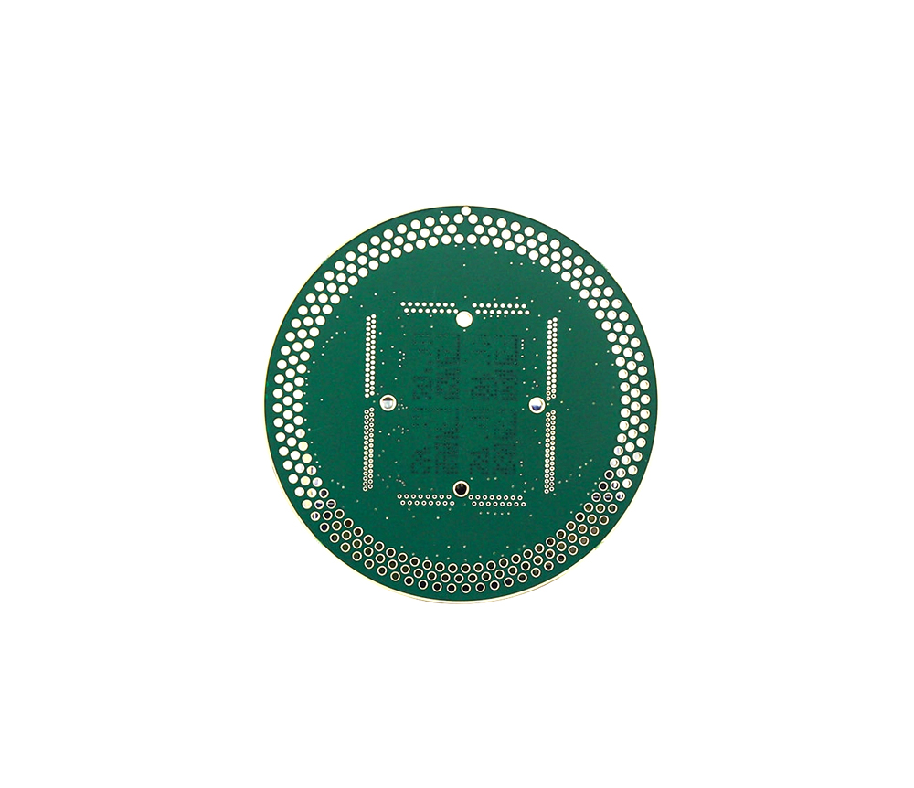
PCB production process Dual -panel system Open → Drilling → PTH → Electroplating → Pre -processing → Dry Film → Pickup → Exposure → Graph Electroplating → Dalf Meeting → Putting Dry Film → Displaying Disposal → Etancular → During Mask → Surface Treatment → Paste the cover film → suppress → curing → nickel gold → printing characters → cutting → electrical test → final inspection → packaging → shipment One -scale Open → Drilling → Patching dry film → Division → Exposure → Evidence → Decoration → Surface treatment → Patch covering film → curing → surface treatment → sinking gold → printing character → electrical test → rushing → rushing Cut → final inspection → packaging → shipment
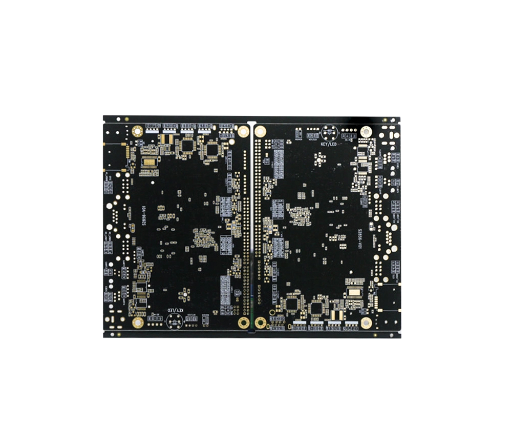
The effect of the wiring of the pad connection and the position of the pores on SMT production: The wiring of the pad connection and the position of the pores has a great impact on the welding rate of SMT, because the inappropriate pad pad connection line and the pores may play the role of "theft" solder. Walk (the rainbow suction and capacity in the fluid). The following situation is good for production quality: 1. Reduce the width of the pad connection line: If there is no current bearing capacity and limitation of PCB manufacturing dimensions, the maximum width of the pad connection line is 0.4mm or 1/2 pile width, which can be smaller. 2. The most preferably selected between the pads connected to the large -scale conductivity belt (such as ground floor, power surface) is a narrow connection line with a length of not less than 0.5mm (the width is not greater than 0.4mm or the width is not greater than 1/2). 3. Avoid introducing pads from the side or corner. The most prefera
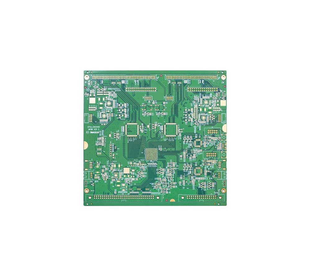
Because the production of the printed circuit board is in the second half of the electronic equipment manufacturing, it has become the downstream industry of the electronics industry. Almost all electronic equipment requires the support of the circuit board. Therefore, printing circuit boards are products with the highest market share in global electronic component products. Japan, China, Taiwan, Western Europe and the United States are the main printed circuit board manufacturing bases. Benefiting from the new products and new market support, the global PCB market has successfully achieved recovery and growth. According to the statistics of the Hong Kong Circuit Board (HKPCA), the global PCB market will develop steadily in 2011, and it is expected to grow by 6-9%, and China is expected to increase by 9-12%. The Taiwan Institute of Technology (IEK) analysis report predicts that the global PCB output value will increase by 10.36%in 2011 to US $ 41.615 billion. According to the rep

The copy plate is removed by a piece of PCB board components, and the surface is clean. We must copy it to the PCB file and follow the steps as follows: 1. Scan the top layer, save the picture, and name top.jpg. At this time, the scanning DPI can be set according to different density. If the settings are 400dpi. 2. Scan the bottom plate, save the picture, and get the name bottom.jpg 3. Make out the middle layer 1 with coarse sandpaper, leak the copper skin, clean it after cleaning, and scan the picture, and get the name MID1.JPG 4. Make the middle layer 2 with coarse sandpaper, leak the copper skin, get it clean, and scan the picture. 5. In the Photoshop, adjust each picture horizontally (select the picture to ensure that the picture is level, so that the lines that come out of this look good, and multiple pictures can be easily aligned). It is recommended to make the underlying image horizontal image in order to make the bottom diagram It is the same direction, the upper and
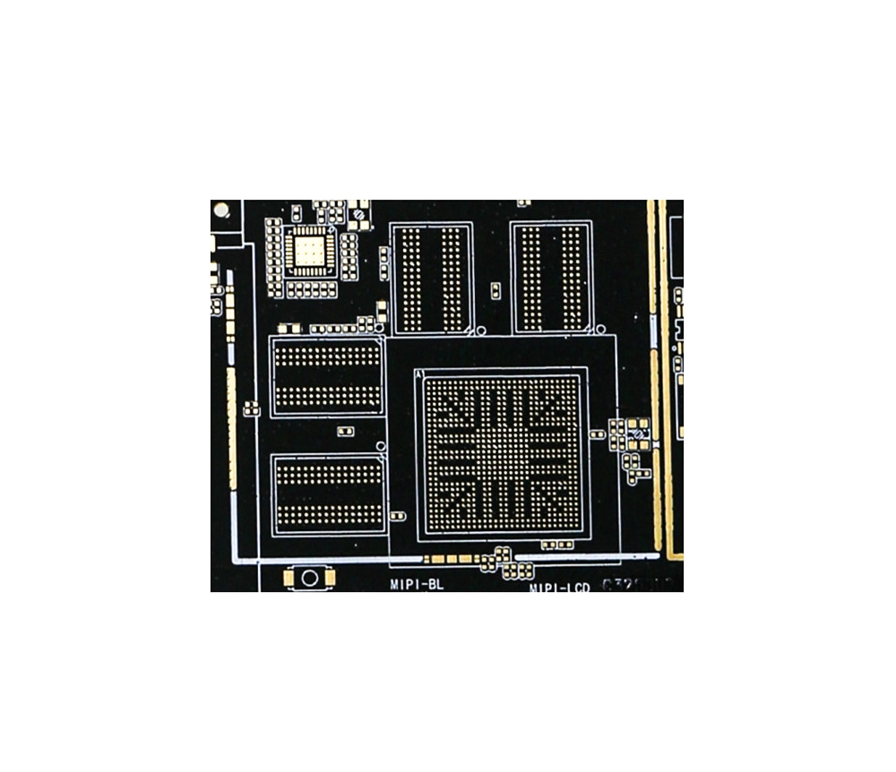
Flexible circuit board (FlexiblePrintedCircuit, FPC), also known as soft circuit board and deflection circuit board, is very popular with excellent characteristics such as light quality, thin thickness, and free bending folding ... It mainly relies on artificial visual inspection, with high cost and low efficiency. With the rapid development of the electronics industry, the design of circuit board design has become more and more high -precision and high density. Traditional artificial testing methods can no longer meet production needs. FPC defect automation testing has become an inevitable trend of industrial development. Flexible circuit (FPC) is a technology developed by the United States to develop aerospace rocket technology in the 1970s. It is a high reliability, excellent deflection made by polycatis film or polytamine as a substrate material. The printing circuit is embedded in the circuit design on the bending light and thin plastic sheet to make a large amount of precisi
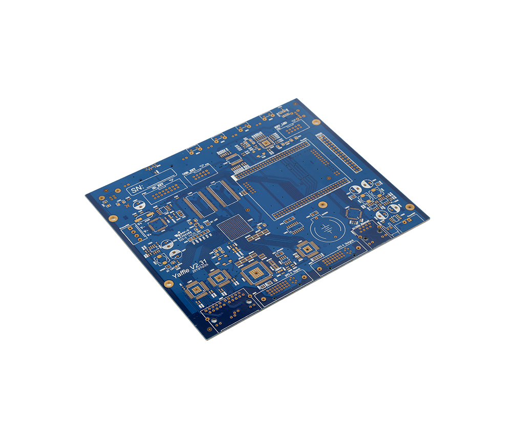
It is composed of a combination bracket, a padding combination plate, a frame support guide system, a material support frame, a unloading device, a cutting knife and its fixing device, an upper plate support system, and a cutting speed changing device. The upper surface of the combination bracket is short, and the padding combination plate is horizontally fixed on the combination bracket. There are slits corresponding to the number of cutting knives on the padding combination plate, The frame support guide system is composed of several pairs of guide sliding devices fixed on the combined bracket and several pairs of positioning devices. The guide sliding devices are fixed on both sides of the combined bracket in pairs, and the positioning devices are also fixed on both sides of the combined bracket in pairs. The material support frame is connected to the frame support guide system in a sliding manner, The guiding sliding device in the frame support and guidance system only allows t
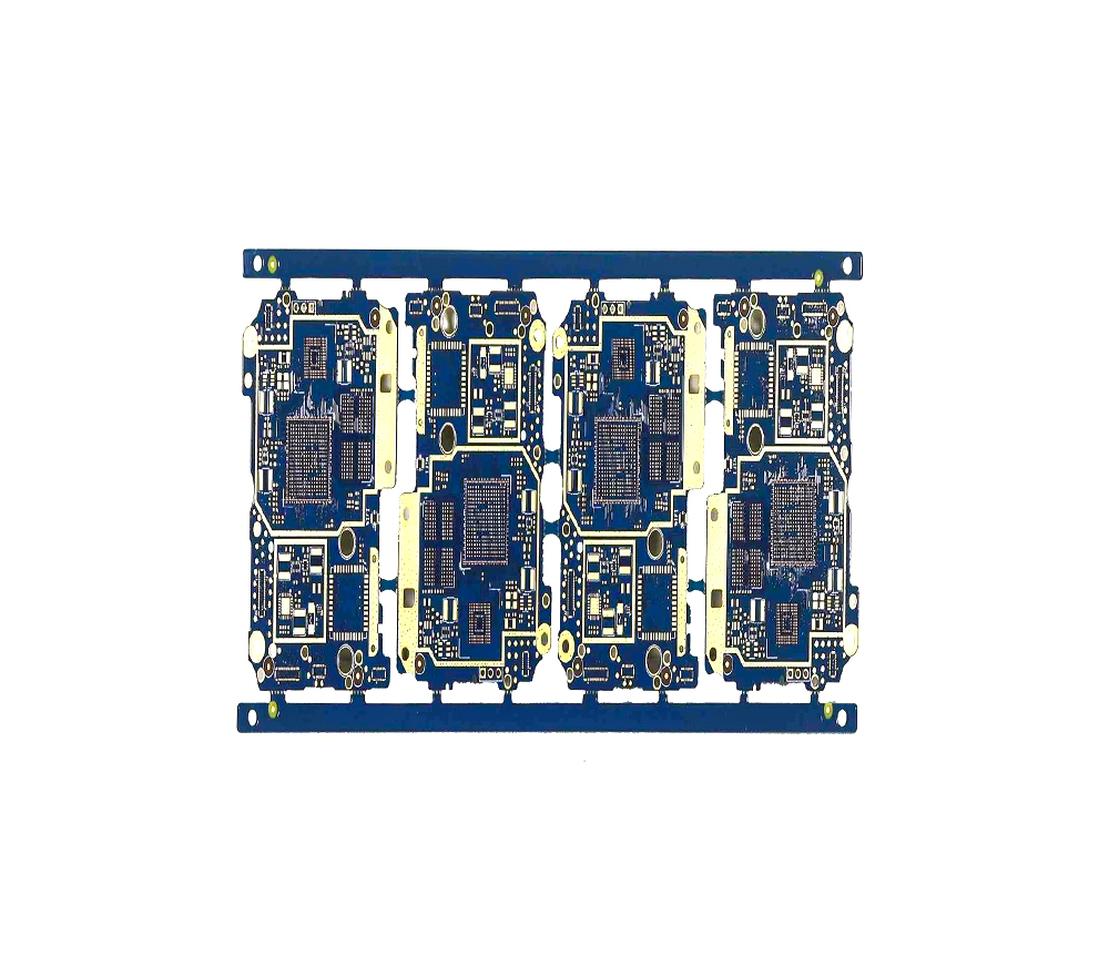
A universal circuit magic board, consisting of a circuit experimental board and circuit components, characterized in that the circuit experimental board (for the sake of specific explanation, electronic circuits are used as examples below) is composed of a double-layer single-sided (or double-sided) printed circuit board of the same size (hereinafter referred to as the printed board), circuit component sockets (such as integrated component sockets, hereinafter referred to as sockets), and pins, A socket is welded into a metalized hole in a printed circuit board that is separated and insulated between the upper and lower layers. On the upper and lower sides centered on the horizontal centerline of the socket, a horizontal line parallel to the horizontal centerline of the socket is printed on the lower layer printed circuit board (or upper layer printed circuit board), and a vertical line perpendicular to the horizontal center of the socket is printed on the upper layer printed circu
Inquiry Now

