 +86 755 2794 4155
  sales@knownpcb.com
-
Shenzhen KNOWNPCB Technology Co., Ltd.
 +86 755 2794 4155
  sales@knownpcb.com
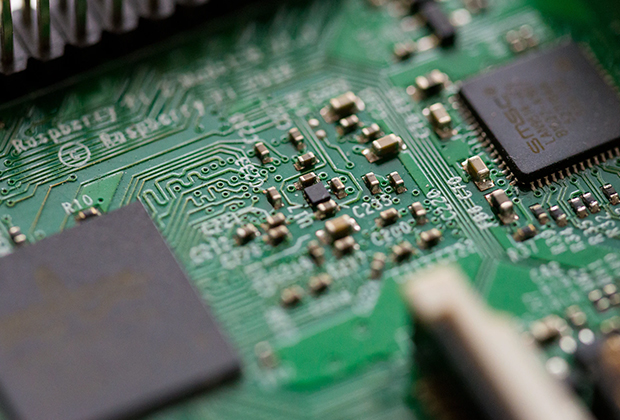
Have you noticed that now more and more of our lighting is using led lighting.What is LED? Compared to the traditional light bulbs, LEDs have lower power consumption, longer lifetime and higher energy efficiency. In the PCB industry,when we say LED PCB, it refers to the pcb used for LED lighting, if you are looking for a suitable LED PCB for your lighting system, this article may bring you something. WHAT ARE LEDS COMPOSED OF?LED is an initial light-emitting diode that produces light when an electric current passes through. LEDs typically have negative and positive electrodes, which generate light in the visible light region.The LEDS are glued to the PCB by soldering process and have electrical connections for lighting.Since light-emitting diodes dissipate a lot of heat when they are in use, when you are designing LED, the metal core is usually the best choice for LED PCB, it is because that it dissipates heat more faster. Among them, the metal material aluminum is the most widely used
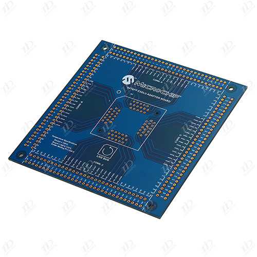
The current trend of electronic products, in a small component or whole machine, constantly integrates more and more devices and functions. Hybrid integration technology has become one of the key technologies that increase the packaging density of source and passive devices. In the mixed integration of various manufacturing steps, the device and the circuit are interconnected, some passive devices such as resistors, such as resistors, are directly made of thick film or film process on the substrate. There are many important parameters of the design of the layout of the mixed integrated circuit board; the width of the wires, the routing of the wire and the keyboard, the height of the bonding coincidence, the height of the bonding leader, and the heat consumption must be considered. The thick -membrane integrated circuit process, the interconnection between the device and the circuit, the wires and resistors are on the substrate, and the various functional pulp is printed and sinte
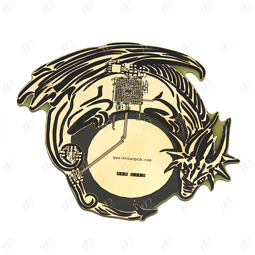
Over the years, the industry is committed to developing the advantages of hybrid integration circuit technology, but has not made a breakthrough in manufacturing costs. Therefore, the printed board assembly process is still the best choice in the complex circuit installation. It is undoubtedly easy to improve the connection process on the naked chip board to make a directly -connected key on the nude chip board. The COB chip direct -board assembly technology is first used for digital clocks, watches. Each printed and circuit board is equipped with a chip, which is now widely used in digital cameras, calculators, telephone cards and various smart cards. Cob is complexCircuit components are equipped with a printer module of 5,000 LEDs and IC -driven combinations. Advanced data processing circuit 32BithP9000 computer motherboard installation 22 ICs and one MODEM circuit and other products have expanded their applications. Today, the multi -chip process with more than 100 chips in a
The current trend of electronic products, in a small component or whole machine, constantly integrates more and more devices and functions. Hybrid integration technology has become one of the key technologies that increase the packaging density of source and passive devices.In the mixed integration of various manufacturing steps, the device and the circuit are interconnected, some passive devices such as resistors, such as resistors, are directly made of thick film or film process on the substrate. There are many important parameters of the design of the layout of the mixed integrated circuit board; the width of the wires, the routing of the wire and the keyboard, the height of the bonding coincidence, the height of the bonding leader, and the heat consumption must be considered.The thick -membrane integrated circuit process, the interconnection between the device and the circuit, the wires and resistors are on the substrate, and the various functional pulp is printed and sintered. The
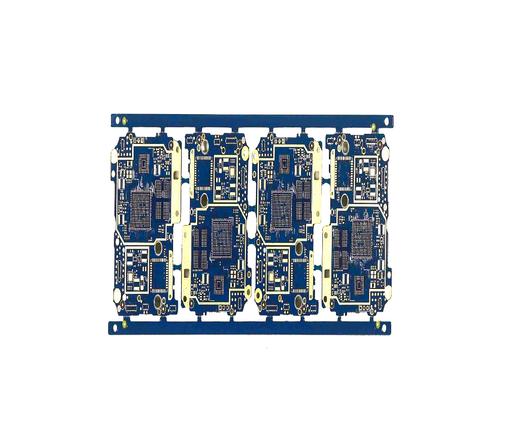
In the process of PCB connection, the traditional manual folding board is used. Although the timeliness is fast, the differences in the power of the manual folding and the position of the angle of the folding board are often caused. The destruction of the road is given this, the PCB fully automatic section machine, the latest gas and electrical lightweight design is used to complete the cutting stress cutting itinerary at one time, which is especially suitable for cutting precision SMD or thin plates. Bowwaves and microcrack are used to use the wedge -shaped tool linear plate to minimize the shear stress, so that the sensitive SMD components, and even the capacitance can not be affected, and the potential quality risk of the product is minimized. The cutting itinerary is below 1-2mm, and there is no concern for operational safety. The knife is made of high-speed steel precision grinding. It can be repeatedly grinded and used for thin plates without V-CUT. SMT production process is
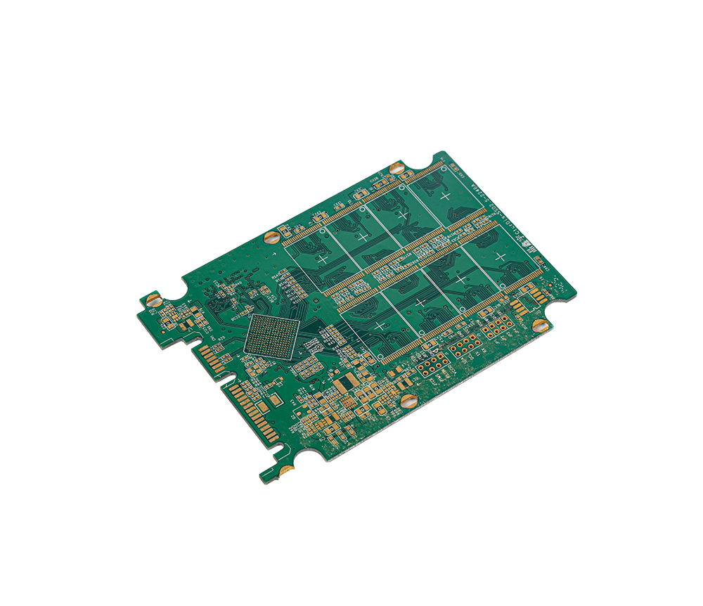
QFN (QUAD FLAT no-Leadpackage, square flat without quotes), one of the surface packaging packaging. Most of them are now called LCC. QFN is the name stipulated by the Japanese Electronic Machinery Industry Association. The enclosure is equipped with an electrode contact. Because there is no pitch, the stickers are smaller than QFP and the height is lower than QFP. However, when the printed substrate and the package are generated, it cannot be relieved at the electrode contact. Therefore, the electrode contact is difficult to get the pins of QFP, generally from 14 to 100. There are two types of materials: ceramics and plastic. When there are LCC marks, they are basically ceramic QFN. The center of the electrode contact is 1.27mm. Plastic QFN is a low -cost packaging of glass epoxy resin printing substrate substrate. In addition to 1.27mm, there are two types: 0.65mm and 0.5mm. This packaging is also called plastic LCC, PCLC, P-LCC, etc.
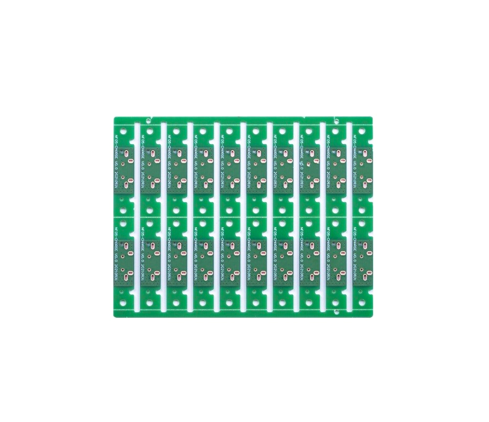
QFN packaging has excellent thermal performance, mainly because there is a large area of heat dissipation pads at the bottom of the packaging. In order to effectively transmit heat from the chip to PCB, the bottom of the PCB must be designed with the corresponding heat dissipation pads and heat dissipation. The heat dissipation pads provide a reliable welding area, and the perfunction provides heat dissipation channels. The size of the heat dissipation pads is at least matched with the exposure of the component. However, various other factors are needed, such as avoiding bridges with the peripheral pads. The amount and size of the heat dissipation depends on the application of the package, the size of the chip power, and the electrical performance requirements. It is recommended that the distance between heat dissipation is 1.0mm to 1.2mm, and the size of the perforated is 0.3mm to 0.33mm. There are four design forms of heat dissipation over -the -pels: such as using a dry membran
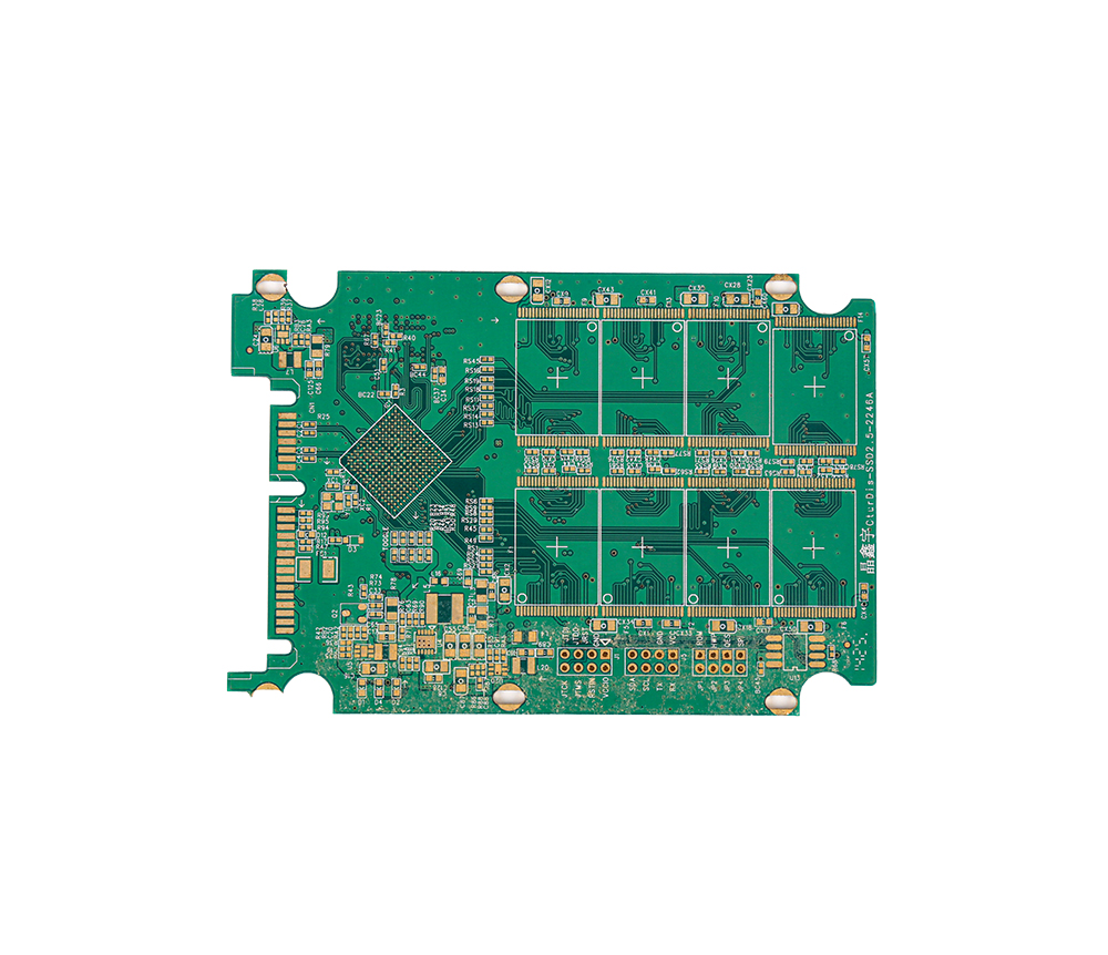
PCB bare board is the abbreviation of Printed Circuit Board. The Chinese name is printed circuit board, also known as print circuit board, printed circuit board. It is an important electronic component, a support body for electronic components, and a provision of electronic components electrical connection. By. Because it is made of electronic printing, it is called a "print" circuit board. As electronic devices are becoming more and more complicated, there are naturally more and more parts required, and the lines and parts on the PCB are becoming more and more dense. Naked plates (there are no parts on it) are often called "printing line board Printed Wiring Board (PWB)". The substrate of the board itself is made of insulation and insulation, and it is not easy to bend the material. The small line materials that can be seen on the surface are copper foil. The originally copper foil was covered on the entire board, and part of the part was carved during the manufacturing process.
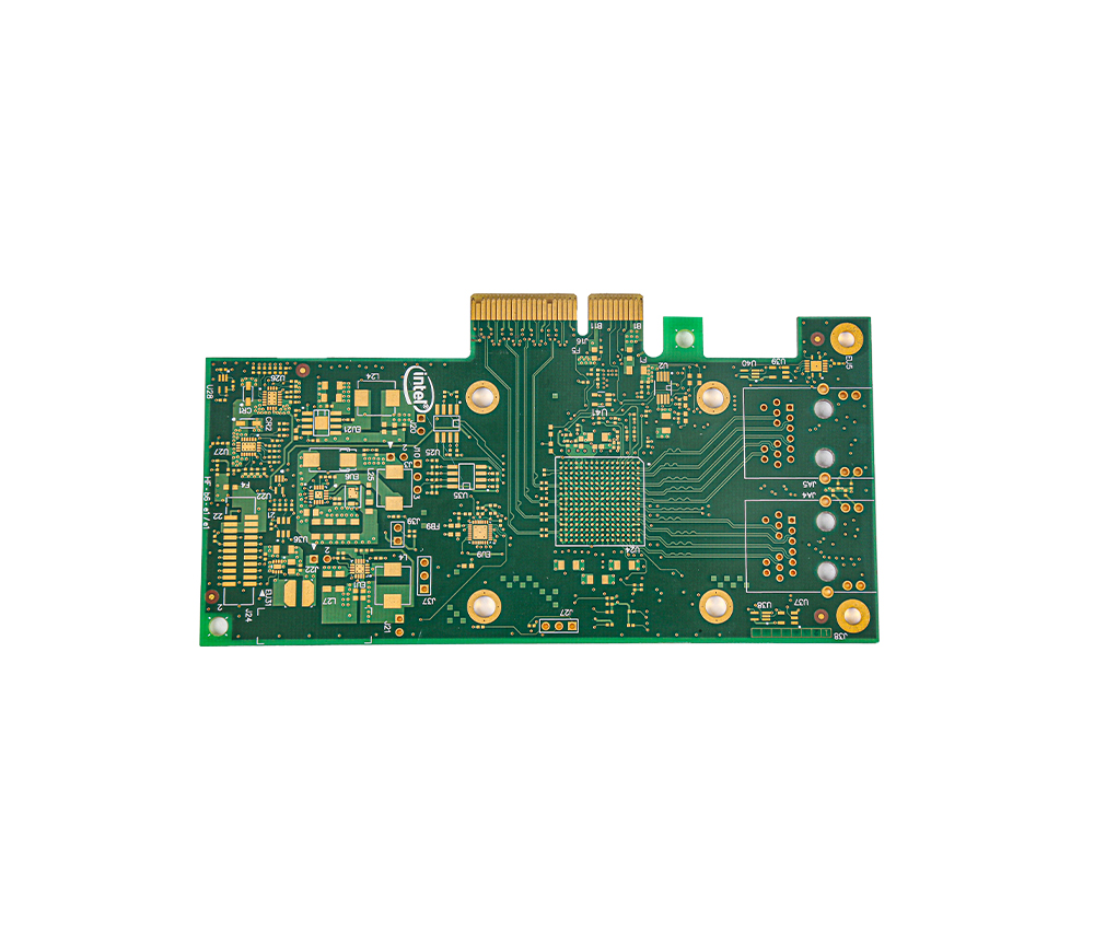
1. There are many dedicated PCB drawing software, such as Protel, etc., you can draw a multi -layer (including double -sided) circuit board diagram. The line is connected to achieve cross -wiring to facilitate typesetting. After the typesetting is completed, it can be handed over to the circuit board of a specific circuit. 2. The double -sided circuit board should be drawn into a circuit schematic in turn, which can be divided into two steps. Step 1: First, draw the symbols of the main components such as IC, etc. The position of the circuit board is drawn on the paper, and the connecting lines and peripheral components are appropriately decorated and drawn to complete the sketch. Step 2: Analyze the principle and organize the circuit diagram according to the habit of drawing. You can also use the circuit schematic diagram software to connect the components and then use its automatic typesetting function to organize. The lines on both sides of the double panel should be accurately
Inquiry Now

